Download
1 / 20
200 likes | 455 Views
A high-performance Silicon Tracker for the CBM experiment at FAIR. J.M. Heuser, W. M ü ller, P. Senger (GSI Darmstadt) C. M ü ntz, J. Stroth (University of Frankfurt) for the CBM Collaboration PANIC05 – Santa Fe, New Mexico, October 2005. Overview:

E N D
A high-performance Silicon Tracker for the CBM experiment at FAIR J.M. Heuser, W. Müller, P. Senger (GSI Darmstadt)C. Müntz, J. Stroth (University of Frankfurt) for the CBM Collaboration PANIC05 – Santa Fe, New Mexico, October 2005 • Overview: • The future accelerator facility FAIR in Darmstadt • The Compressed Baryonic Matter experiment • The CBM Silicon Tracker • Performance requirements • Detector concept • R&D directions J.M. Heuser et al. CBM Silicon Tracker
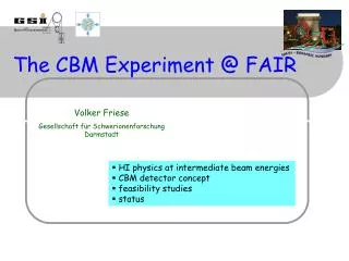
Facility for Antiproton and Ion Research • FAIR: Future international accelerator complex at GSI, Darmstadt, Germany • Research program includes physics with: • Radioactive ion beams: Structure of nuclei far from stability • Anti-proton beams: Hadron spectroscopy, anti hydrogen • Ion and laser induced plasmas: High energy density in matter • High-energy nuclear collisions: Strongly interacting matter at high baryon densities Project Management: Start of construction: 2007/2008 First beams: 2011 Full operation, CBM: 2015 see talk of L. Schmitt max. U: 35 GeV/n p: 90 GeV Heavy-ion synchrotrons SIS 100 SIS 300 UNILAC Compressed Baryonic Matter Experiment J.M. Heuser et al. CBM Silicon Tracker
CBM - Physics Motivation Strong-interaction physics: confinement, broken chiral symmetry, hadron masses. CERN-SPS and RHIC: indications for a new state of matter: „Quark Gluon Plasma“. Produced at high T and low B. LHC: even higher T, lower B. QCD phase diagram: poorly known at low T, high B: new measurements at FAIR: with highest baryon densities, and with new probes! CBM Experiment J.M. Heuser et al. CBM Silicon Tracker
Physics and Observables Open charm measurement: One of the prime interests of CBM, one of the most difficult tasks! • Tracking challenge: • up to 107 Au+Au reactions/sec @ 25 GeV/nucleon • ~ 1000 charged particles/event, up to ~100 tracks/cm2/event • momentum measurement with resolution < 1% • secondary vertex reconstruction ( 30 m) • high speed data acquisition and trigger system URQMDAu+AU 25 GeV/nucleon J.M. Heuser et al. CBM Silicon Tracker
The CBM Experiment- Conceptional Design - • Tracking, momentum measurement, vertex reconstruction: Exclusively with a Silicon Tracking System (STS) • Electron ID: RICH & TRD (& ECAL) • Hadron ID: TOF (& RICH) • Photons, p0, m: ECAL • High interaction rates • No central trigger • Data-push r/o architecture ECAL (12 m) RICH magnet beam target STS (5, 10, 20, 40, 60, 80, 100 cm) TOF (10 m) Further specific detector configurations under study. TRDs (4,6, 8 m) J.M. Heuser et al. CBM Silicon Tracker
Assume 7 planes 2 or 3 thin pixel stations: secondary vertex detection (benchmark: open charm) 4 or 5 thin strip stations: tracking Acceptance: 50 to 500 mrad First plane: z=5cm ; size 25 cm2 Last plane: z=100cm; size ~1 m2 Magnetic dipole field: ~ 1Tm, p/p <1% @ p=1 GeV 7 6 tracking 5 4 pixel detectors strip detectors vertexing 3 2 1 vacuum z = 5,10,(20) cm z = (20),40,60,80,100 cm The Silicon Tracking System - Conceptional Geometry - J.M. Heuser et al. CBM Silicon Tracker
D0→K-+ primary tracks c target Challenge: Open Charm Reconstruction Some hadronic decay modes: D(c = 317 m): D+ K-++ (9 0.6%) D0(c = 124.4 m): D0 K-+(3.9 0.09%) High-granularity sensors. Thin tracking stations. Rare probe: High level charm trigger. J.M. Heuser et al. CBM Silicon Tracker
Primary vertex resolution 100 µm thick MAPS 25x25 µm2 = 5.3 µm Hybrid 35x35 µm2 = 8.0 µm Hybrid 350x50 µm2 = 50 µm 750 µm thick 750 µm thick MAPS (25x25 µm2) 10% eff. HYBRID (35x35 µm2) 1.7% eff. HYBRID (350x50 µm2) 0.01% eff. D0 vertex resolution with MAPS single-track impact parameter cut yielding same background rejection. Pixel Detectors for Vertexing What kind of pixel detectors can do the job? Study of different detector types, characterized by their material budgets and pixel sizes: D0 impact parameter measurement MAPS 25x25 µm2100 µm thick = 38 µm = 38 µm I. Vassiliev et al., GSI small pixels ≤ 25 x 25 µm2 ( thin sensors ~ 100 µm ) J.M. Heuser et al. CBM Silicon Tracker
D0K-,+signal Background Reconstructed events Z-vertex (cm) Rate 106 interactions/s HYBRID 35 x 35, 750 µm D0→ K-π+ reconstruction using MAPS Signal Cuts ~10 % efficiency study by I. Vassiliev, GSI J.M. Heuser et al. CBM Silicon Tracker
Pixel Detector Requirements • Small pixels – less than 25 x 25 µm2 • Thin – less than ~100 µm silicon • Radiation hard > 1014 nequiv/cm2 • Fast readout – interaction rate up to 107/s Such a detector does not exist ! Two possible R&D directions: Monolithic Active Pixel Sensors (MAPS): - small pixels: 25 x 25 µm2 - thin: standard 120 µm; study: 50 µm - spatial resolution: ~3 µm - too slow for CBM: ~ms/Mpixel full frame - limited rad. hardness (bulk damage) Improve r/o time, radiation tolerance. Hybrid Pixel Detectors (LHC type): - fast readout - radiation hard - too large pixels: 50 x ~400 µm2- spatial resolution: ~15 (115) µm - thick: standard > 350 µm Reduce pixel size and thickness. We started persuing the MAPS option, together with IReS Strasbourg.Alternative to consider: DEPFET sensors (MPI Munich). J.M. Heuser et al. CBM Silicon Tracker
R&D goals with MAPS: Radiation tolerance & readout speed R&D goals with MAPS: radiation tolerance: ~1012 1013 1 MeV nequiv. readout time: 10 sec, column parallel r/o, in reach in next years Expected situation in CBM: Fluence at 1st MAPS station: ~10 1-MeV nequiv. per event detector partly destroyed after 1012 reactions corresponds to 105 D mesons detected (decent measurement!) Possible running conditions: a)1 day detector lifetime at 107 reactions/s,100 events piled up, or b) 4 month detector lifetime at 105 reactions/s, no pile-up events. URQMD, Au+Au 25 GeV/nucleon Fluence of 1 MeV nequiv./cm2in 1st MAPS station at z = 5cm Kpn Consider also future developments: Hybrid pixels ~ 50x50 µm2, few hundred µm thick, with higher radiation tolerance and faster readout. J.M. Heuser et al. CBM Silicon Tracker
Tracking in Silicon Strip Stations First attempts:Problem - High occupancy with many combinatorial hit points in silicon strip stations. Recent approach:Cellular automaton technique: Works! Example:4 strip stations + 3 MAPS stations MAPS pile-up: 10 events I. Kisel, Heidelberg, and S. Gorbunov, DESY J.M. Heuser et al. CBM Silicon Tracker
Tracking Requirements Tracking with microstrip and pixel stations: Works despite of combinatorial hits and pile-up! But: Noise, misalignment, detector inefficiencies etc. not taken into account! Consider more tracking redundancy! Comprehensive study on the way to optimize the Silicon Tracker's layout, including: - more tracking stations, - several strip geometries, - additional (hybrid?) pixel detectors supporting the tracking, and - detailed modeling of the detectors. J.M. Heuser et al. CBM Silicon Tracker
Pixel Detector – Module Concept CMOS MAPS chips for CBM: - size: ~0.5 x 1 cm2- ~50% sensor, ~50% r/o.- column readout in ~10 µs CBM MAPS ladders with 4 or 5 "chips". Detector module: BTeV inspired design ladders mounted on either side of a substrate providing (active?) cooling. Active cooling support: a carbon fiber structure with micro pipes? ~ 0.3% X0 glass or silicon wafers with buried micro channels? ~ 0.1-0.3% X0 J.M. Heuser et al. CBM Silicon Tracker
Strip Detector – Modules & Stations Four detector stations: built from a few wafer types. Basic sensor elements: 200 m thick silicon wafers. double-sided, rad-tolerant. 50 m (25 m?)strip pitch. Inner : 6x4 cm Middle : 6x12 cm Outer : 6X20 cm Study of: • strip length, pitch, stereo angle(to reduce fake hits) • single-sided sensor option • location of read-out chips(on sensor / outside acceptance) J.M. Heuser et al. CBM Silicon Tracker
Summary CBM – High-rate fixed-target heavy-ion experiment planned at FAIR/SIS300. – Strong-interaction physics, high baryon densities: Au+Au up to 35 GeV/nucl. – Challenge: Rare probes - Open charm, low-mass vector mesons di-leptons. Experimental concept, new to heavy-ion physics: – Tracking exclusively with a high-performance Silicon Tracker. – Very important detector system, key to the physics of CBM. Silicon Tracker performance requirements: – Efficient tracking, high momentum resolution. – High-resolution vertexing.Benchmark: Open charm. Small pixels, thin, radiation tolerant, fast r/o. Beyond state-of-the-art! Detector R&D started: – Thin, fine-pitch double-sided microstrip sensors (tracking). – MAPS with improved radiation hardness, readout speed (vertexing). – Readout electronics. Open for new ideas!http://www.gsi.de/fair/experiments/CBM/index_e.html J.M. Heuser et al. CBM Silicon Tracker
Discussion J.M. Heuser et al. CBM Silicon Tracker
Low Mass Dilepton Spectroscopy Background: 0 decay (365/event) 0 e+e- (1.2%) 0 98.8%) conversion e+e- Signal:vector meson decays , , e+e- • Detector requirements: • first stations with large acceptance • tracking efficiency down to p = 0.1 GeV/c to suppress background • detect conversion pairs: → small pixels ... fake open pair is formed. If missed ... J.M. Heuser et al. CBM Silicon Tracker
Delta Electrons hits in 1st MAPS station:1000 min. bias URQMD events, Au+Au 25 AGeV. • Beam ions on target: • produce delta-rays dominate occupancy when integrated over many events. • high local radiation damage, comparable to bulk damage. hits spoil track finding • limits rate capability • Only way out: Fast detector readout to avoid electron hit pile-up. study by I. Vassiliev, GSI J.M. Heuser et al. CBM Silicon Tracker
Data-Push Architecture, Data Flow • Each detector channel detects autonomously all hits FEE design. • An absolute time stamp, precise to a fraction of the sampling period, is associated with each hit. • All hits are shipped to the next layer (usually data concentrators). • Association of hits with events done later using time correlation. Typical parameters: (few % occupancy, 107 interaction rate) • some 100 kHz hit rate per channel • few MByte/sec per channel • whole CBM detector: ~ 1 Tbyte/sec J.M. Heuser et al. CBM Silicon Tracker