Download
1 / 14
140 likes | 283 Views
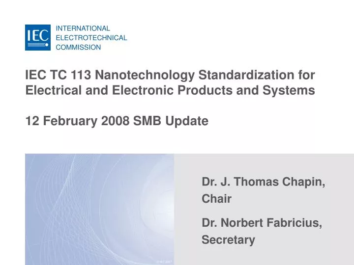
IEC TC 113 Nanotechnology Standardization for Electrical and Electronic Products and Systems 12 February 2008 SMB Update. Dr. J. Thomas Chapin, Chair Dr. Norbert Fabricius, Secretary. Scope and SPS of IEC TC113.

E N D
IEC TC 113 Nanotechnology Standardization for Electrical and Electronic Products and Systems12 February 2008 SMB Update Dr. J. Thomas Chapin, Chair Dr. Norbert Fabricius, Secretary
Scope and SPS of IEC TC113 Standardization of the technologies relevant to electrical and electronic products and systems in the field of nanotechnology in close cooperation with other IEC committees and ISO TC 229. • Components / intermediate assemblies created from nano-scaled materials and processes. • Properties and functionalities of these components / intermediate assemblies are electrical or electro-optical. • Final products using these components / intermediate assemblies are typically within the scope of other IEC TC's • Fields of activities are for example: • electronics, • optical aspects addressed by IEC TC’s, • magnetics and electromagnetics, • electroacoustics, • multimedia and telecommunication, • energy production (direct conversion into electrical power like in fuel cells, photovoltaic devices, storage of electrical energy). • Specific topics: Terminology, measurement, characterization, performance, reliability and safety and environment related to the nanoscale.
IEC TC 113 Membership 14 Participating Members– 14 Observing Members EGYPT ESTONIA FINLAND FRANCE GERMANY GREECE HUNGARY ICELAND (AM) INDIA INDONESIA IRAN IRELAND ISRAEL ITALY JAPAN KAZAKHSTAN (AM) KENYA (AM) KOREA, DPR OF (AM) KOREA, REP OF LATVIA (AM) LITHUANIA (AM) LUXEMBURG MACEDONIA (AM) MALAYSIA MALTA (AM) MEXICO NETHERLANDS NEW ZEALAND NIGERIA (AM) NORWAY PAKISTAN POLAND PORTUGAL ROMANIA RUSSIAN FED SAUDI ARABIA SERBIA & MONTENEGRO SINGAPORE SLOVAKIA SLOVENIA SOUTH AFRICA SPAIN SRI LANKA (AM) SWEDEN SWITZERLAND THAILAND TUNISIA (AM) TURKEY UKRAINE UK USA VIETNAM (AM) ARGENTINA AUSTRALIA AUSTRIA BELARUS BELGIUM BOSNIA-HERZEGOVINA BRAZIL BULGARIA CANADA CHINA COLOMBIA (AM) CROATIA CYPRUS (AM) CZECH REP DENMARK
International Standardisation in Nanotechnology TC47 IEC TC's SEMI TC86 D-liaison TC111 IEEE A-liaison D-liaison IEC TC 113 ISO TC 229 WG3: Performance assessment WG3: Health, safety environment Appointed Observer JWG1: Terminology, nomenclature JWG2: Measurement, characterization D-Liaisons: SEMI and IEEE (under SMB ballot)
Working Group Structure of IEC TC113 • JWG 1: "Terminology and Nomenclature" • Scope: Define and develop unambiguous and uniform terminology and nomenclature in the field of nanotechnologies to facilitate communication and to promote common understanding. • JWG 2: "Measurement and Characterization" • Scope: Standardization of metrology and test methods and consideration of reference materials used to characterize properties of mainly materials and structures in the field of nanotechnologies. • WG 3: "Performance assessment" • Scope: To develop standards for the assessment of performance, reliability, and durability related to the nanotechnology-enabled aspects of components and systems in support of continuous improvement at all stages of the value adding chain.
Liaison between IEC TC113 and ISO TC229 • Every two years there will be a co-allocated plenary meeting to improve networking between the TC’s. • Chairman and Secretary attend the plenary meetings of the other committee. • Two Joint Working Groups with Convener and Co-Convener from both TC’s. • Regular consultancy of the officers of both TC’s. • Common IEC/ISO standards with coordinated voting are under consideration. • Common workshops will take place (e.g. 26.2.2008 - 28.2.2008, Gaithersburg, NIST USA).
IEC TC 113 WG3 Programme of Work • Standards to characterize nano-specific product performance • Fast "Screening Methods" to assess reliability and durability • Modelling of nano-related failure mechanisms • Fast standardized test methods for nano fabrication • Identification of "Nano Key Control Characteristics" for Material and Process SPC • Electronic-grade nano materials specifications • Generic nano material specification • Electronic grade CNT specification
Area of Nanotechnology Standardization IEC Product TC's Nano-enabled Product System Integration IEC TC 113 Nano Subassembly Subassembly #1 Subassembly #N Nano Materials & Processes Nano Science
Area of Nanotechnology Standardization KCC – key control characteristics IEC Product TC's Nano-enabled Product KCC‘s System Integration IEC TC 113 Nano Subassembly Subassembly #1 Subassembly #N Nano Materials & Processes Nanoscale Driven Failure Modes Nano Science
Area of Nanotechnology Standardization Nano-enabled Product System Integration Nano Subassembly Subassembly #1 Subassembly #N Carbon nanotube Nano Materials & Processes Prof. Young Hee Lee, Sungkyunkwan University, KO Samsung Nano Science KCC – key control characteristics
Area of Nanotechnology Standardization Nano-enabled Product System Integration Nano Subassembly Subassembly #1 Subassembly #N Nano Materials & Processes Nano Science
IEC TC 113 Working Activities New Work Items: • IEC/TC 113/WG3 - Specification for Carbon Nanotube Characteristics for Electrotechnical Applications Meeting History: • IEC TC 113: 26-27 March 2007 in Frankfurt (1st TC 113 Plenary) • IEC TC 113/WG3 20-21 July 2007 in San Francisco • IEC TC 113: 04-07 December 2007 in Singapore (2nd TC 113 meeting, co-located with ISO/TC 229) • IEC TC 113/WG3: 08 April 2008 in Tokyo • IEC TC 113: 11-13 November 2008 in US (3rd TC 113 Plenary)
Summary • IEC TC 113 is now active and has held 2 plenary meetings. • IEC TC 113 has established a strategic liaison with ISO TC 229. • Pursuing liaisons with other organizations involved in nanotechnology (SEMI, IEEE). • IEC TC 113 and ISO TC 229 have two Joint Working Groups with parallel activities. • IEC TC 113 WG3 has been established and now working on specific work items.
Summary, cont’d. • IEC TC 113 is actively recruiting technical experts for working group activities. • IEC TC 113 developing an international survey on nanotechnology to help guide focus and priority. • IEC TC 113 created and staffed a Chairman’s Advisory Group (CAG) to help facilitate strategic and tactical planning for the TC. CAG composed of IEC TC 113 leadership plus 1 nominated representative from each NC.