Download
1 / 42
470 likes | 1.2k Views
Diffusion #1. ECE/ChE 4752: Microelectronics Processing Laboratory. Gary S. May January 29, 2004. Outline. Introduction Apparatus & Chemistry Fick’s Law Profiles Characterization. Definition.

E N D
Diffusion #1 ECE/ChE 4752: Microelectronics Processing Laboratory Gary S. May January 29, 2004
Outline • Introduction • Apparatus & Chemistry • Fick’s Law • Profiles • Characterization
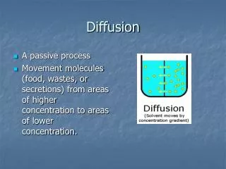
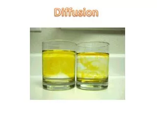
Definition • Random walk of an ensemble of particles from regions of high concentration to regions of lower concentration • In general, used to introduce dopants in controlled amounts into semiconductors • Typical applications: • Form diffused resistors • Form sources/drains in MOS devices • Form bases/emitters in bipolar transistors
Basic Process • Source material transported to surface by inert carrier • Decomposes and reacts with the surface • Dopant atoms deposited, dissolve in Si, begin to diffuse
Outline • Introduction • Apparatus & Chemistry • Fick’s Law • Profiles • Characterization
Dopant Sources • Inert carrier gas = N2 • Dopant gases: • P-type = diborane (B2H6) • N-Type = arsine (AsH3), phosphine (PH3) • Other sources: • Solid = BN, As2O3, P2O5 • Liquid = BBr3, AsCl3, POCl3
Solid Source Example reaction: 2As2O3 + 3Si → 4As + 3SiO2 (forms an oxide layer on the surface)
Liquid Source • Carrier “bubbled” through liquid; transported as vapor to surface • Common practice: saturate carrier with vapor so concentration is independent of gas flow • => surface concentration set by temperature of bubbler & diffusion system • Example: 4BBr3 + 3O2→ 2B2O3 + 6Br • => preliminary reaction forms B2O3, which is deposited on the surface; forms a glassy layer
Gas Source • Examples: • a) B2H6 + 3O2→ B2O3 + 3H2O (at 300 oC) • b) i) 4POCl3 + 3O2→ 2P2O5 + 6Cl2 • (oxygen is carrier gas that initiates preliminary reaction) • ii) 2P2O5 + 5Si → 4P + 5SiO2
Outline • Introduction • Apparatus & Chemistry • Fick’s Law • Profiles • Characterization
Diffusion Mechanisms • Vacancy: atoms jump from one lattice site to the next. • Interstitial: atoms jump from one interstitial site to the next.
Vacancy Diffusion • Also called “substitutional” diffusion • Must have vacancies available • High activation energy (Ea ~ 3 eV hard)
Interstitial Diffusion • “Interstitial” = between lattice sites • Ea = 0.5 - 1.5 eV easier
First Law of Diffusion • F = flux (#of dopant atoms passing through a unit area/unit time) • C = dopant concentration/unit volume • D = diffusion coefficient or diffusivity • Dopant atoms diffuse away from a high-concentration region toward a lower-concentration region.
Conservation of Mass • 1st Law substituted into the 1-D continuity equation under the condition that no materials are formed or consumed in the host semiconductor
Fick’s Law • When the concentration of dopant atoms is low, diffusion coefficient can be considered to be independent of doping concentration.
Temperature Effect • Diffusivity varies with temperature • D0 = diffusion coefficient (in cm2/s) extrapolated to infinite temperature • Ea = activation energy in eV
Outline • Introduction • Apparatus & Chemistry • Fick’s Law • Profiles • Characterization
Solving Fick’s Law • 2nd order differential equation • Need one initial condition (in time) • Need two boundary conditions (in space)
Constant Surface Concentration • “Infinite source” diffusion • Initial condition: C(x,0) = 0 • Boundary conditions: C(0, t) = Cs C(∞, t) = 0 • Solution:
Key Parameters • Complementary error function: • Cs = surface concentration (solid solubility)
Total Dopant • Total dopant per unit area: • Represents area under diffusion profile
Example For a boron diffusion in silicon at 1000 °C, the surface concentration is maintained at 1019 cm–3 and the diffusion time is 1 hour. Find Q(t) and the gradient at x = 0 and at a location where the dopant concentration reaches 1015 cm–3. SOLUTION: The diffusion coefficient of boron at 1000 °C is about 2 × 1014 cm2/s, so that the diffusion length is
Example (cont.) When C = 1015 cm–3, xj is given by
Constant Total Dopant • “Limited source” diffusion • Initial condition: C(x,0) = 0 • Boundary conditions: C(∞, t) = 0 • Solution:
Example Arsenic was pre-deposited by arsine gas, and the resulting dopant per unit area was 1014 cm2. How long would it take to drive the arsenic in to xj = 1 µm? Assume a background doping of Csub = 1015 cm-3, and a drive-in temperature of 1200 °C. For As, D0 = 24 cm2/s and Ea = 4.08 eV. SOLUTION:
Example (cont.) t • log t – 10.09t + 8350 = 0 • The solution to this equation can be determined by the cross point of equation: y = t • log t and y = 10.09t – 8350. • Therefore, t = 1190 seconds (~ 20 minutes).
Pre-Deposition • Pre-deposition = infinite source xj = junction depth (where C(x)=Csub)
Drive-In • Drive-in = limited source • After subsequent heat cycles:
Multiple Heat Cycles where: (for n heat cycles)
Outline • Introduction • Apparatus & Chemistry • Fick’s Law • Profiles • Characterization
Junction Depth • Can be delineated by cutting a groove and etching the surface with a solution (100 cm3 HF and a few drops of HNO3 for silicon) that stains the p-type region darker than the n-type region, as illustrated above.
Junction Depth • If R0 is the radius of the tool used to form the groove, then xj is given by: • In R0 is much larger than a and b, then:
4-Point Probe • Used to determine resistivity
4-Point Probe 1) Known current (I) passed through outer probes 2) Potential (V) developed across inner probes r = (V/I)tF where: t = wafer thickness F = correction factor (accounts for probe geometry) OR: Rs = (V/I)F where: Rs = sheet resistance (W/) => r = Rst
Resistivity where: s = conductivity (W-1-cm-1) • r = resistivity (W-cm) • mn = electron mobility (cm2/V-s) • mp = hole mobility (cm2/V-s) • q = electron charge (coul) • n = electron concentration (cm-3) • p = hole concentration (cm-3)
Sheet Resistance • 1 “square” above has resistance Rs (W/square) • Rs is measured with the 4-point probe • Count squares to get L/w • Resistance in W = Rs(L/w)
Sheet Resistance (cont.) • Relates xj, mobility (m), and impurity distribution C(x) • For a given diffusion profile, the average resistivity ( = Rsxj) is uniquely related to Cs and for an assumed diffusion profile. • Irvin curves relating Cs and have been calculated for simple diffusion profiles.