Download
1 / 59
590 likes | 686 Views
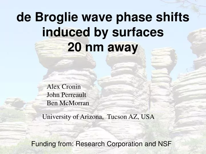
de Broglie wave phase shifts induced by surfaces 20 nm away. Alex Cronin John Perreault Ben McMorran. University of Arizona, Tucson AZ, USA. NSF. Funding from: Research Corporation and NSF. Outline:. Nano-Structure Gratings. Coherent effects of V vdW (r)=C 3 /r 3 on Atom beams

E N D
de Broglie wave phase shifts induced by surfaces 20 nm away Alex Cronin John Perreault Ben McMorran University of Arizona, Tucson AZ, USA NSF Funding from: Research Corporation and NSF
Outline: Nano-Structure Gratings • Coherent effects of VvdW(r)=C3/r3 on Atom beams • Diffraction Intensities |An|2 depend on atom velocity • No missing orders regardless of open fraction • Interferometer measurement of phase shift in 0th order • Measure of phase in 1st and 2nd orders • Electron Optics Experiments on Vimage(r) = C1/r • Asymmetric Diffraction • Depends on incident velocity and angle
x x 0 1 3 2 5 4 6 7 Na Atom Diffraction z 100 nm period diffraction grating 60 μm diameter hot wire detector 10 μm collimating slits .5 mm skimmer supersonic source Atom Flux (kC/s) Detector Position x (mm)
x’ x Na Removable interaction grating Atom Interferometry z 100 nm period diffraction grating 60 μm diameter hot wire detector 10 μm collimating slits .5 mm skimmer supersonic source Atom Flux (kC/s) Atom Flux Grating Position x’ (nm)
Nano-Structure Gratings period d= 100 nm, window size w ~ 50 nm “Large-area achromatic interferometric lithography for 100nm period gratings and grids” T. A. Savas, M. L. Schattenburg, J. M. Carter and H. I. Smith. Journal of Vacuum Science and Technology B 14 4167-4170 (1996)
To understand the role of vdW forces on atom diffraction: • Start with Vvdw in all space • Compute phase shift just after the grating • Propagate to the detector plane
Atom-surface (and electron-surface) interactons cause phase shifts for de Broglie waves that are transmitted through the grating channels. At 10 nm, 3 meV and 0.3 eV but the same f=0.3 rad
Far-Field Diffraction Envelopes for Intensity Note: 2nd order would have p phase shift if C3=0.
Atom phase vdW Potential grating bar grating bar grating bar r1 r2 atom with velocity v
Amplitude and phase of nth order change with C3/velocity Phase shift in nth order.
velocity = 662 m/s velocity = 1091 m/s velocity = 2219 m/s velocity = 3171 m/s
Best Fit to |An|2 with only one free parameter: C3
Rx to determine the strength of the van der Waals potential V(r)=C3r -3: 1. Measure physical grating parameters: w, t, d 2. Fit diffraction pattern to determine flux in each order |An|2 3. Fit |An|2 to determine C3
Systematic Uncertainties Imperfect determination of grating geometry w, t and wedge angle. Uncertainty of 1 nm in w dominates the uncertainty in C3. Lineshape used to fit the raw diffraction pattern Gaussian works poorly, empirical lineshape works better. What is the potential V everywhere in and near the grating? structure is partially coated with sodium Slot walls are not semi-infinite planes NOT YET ADDRESSED
Dirty Gratings Have been Cleaned (AFM images)
Different power-law potentials make distinct diffraction envelopes. V(r) = -Cn/rn Cn chosen to match I1/I0 r=0 n=2 n=3 n=4 n=5
Next: • Rotate the grating through “50% open fraction” • and note second order is never suppressed. • measure absolute transmission into zeroth order • (it should change with C3/velocity) • Use an interferometer to measure phase shift in 0th order • Use different surface coating.
E.g. w/d = 1/3 missing orders ±3, ±6, ... Missing orders would occur when zeros from single-slit diffraction coincide with constructive interference from many-slits.
Experiment 2: Twistthe grating to search for missing orders atom beam detector twist axis
Intensity in Each Order vs. Twist 0th order Model parameters: d=100 nm, w=67 nm, t=116 nm, a= 3.5o. Dashed red lines C3=0 Solid black lines C3=5 meVnm3 1st order 2nd order 3rd order 4th order angle (degrees)
Asymmetric +/- 1 orders
d w l a • Blazed Gratings • for Atom Waves • requirements: • van der Waals j(x) • Asymmetric channel walls 0 Region where df(x)/dx = kjmost strongly affectsjth order
Optical diffraction • Much more symmetric, • missing orders possible • Atom diffraction • Asymmetric, • no missing orders - ever
Theorem: There are no missing orders in atom diffraction from a material grating. Corollary: Atom-surface interactions can be measured by studying atom diffraction.
Vibration curves can prove “No Missing Orders” Thm A way to visualize the cumulative integral for Yn x Y1 2nd w d Arrows from tail to tip represent amplitudes Yn. In =|Yn|2
Vibration Curves Y2 (a) diffraction with absorption only Y2 (b) Van der Waals j(x) included Arrows from tail to tip represent amplitudes Yn. In =|Yn|2
Model shown for: second diffraction order w/d = 0.48 C3 = 0, 1, 10, 100 meVnm3 Unless C3=0, endpoints of the spiral never overlap. Therefore Yn is never zero, i.e., there are never missing orders. Q.E.D.
Expt.#3: Use Diffraction Phase to Measure C3 • Zeroth order intensity and phase depend on the strength of the van der Waals interaction with the grating bars. 0th order transmission vs. C3 phase shift vs. C3
Phase j0 due to Interaction Grating |a> Slits Detector Atom beam |b> Interaction Grating
Preparing an interaction grating to act on one arm of the interferometer Gap Position (mm) In-tact Grating
gap gap gap 1 um In tact grating
A B C B A B Measurement of Phase Shift Induced by the Interaction Grating (raw data 5 sec/ pt) Interaction grating position A B C
Phase Shift Induced by the Interaction Grating (averaged data) • Phase shift induced by grating is φo=.22+/-.03 rad • 90 seconds of data total • C3 = 4.0 +/- 1.0 meV nm3
See talk by John Perreault about the interferometer experiment.
Expt. #4: Measure the far-field f1 and f2 FA FB FC FD L1 L2 Four different interferometers:
Amplitude and phase of nth order change with C3/velocity Velocity / [km/s] Velocity / [km/s]
Contrast from Four interferometers is resolved (thanks to 100 nm period gratings and 2 m IFM)
Predicted Phase shifts in red * * * *= preliminary data
Summary of 4 Experiments Theory Na with core + e=∞ Na valence + e=∞ Na + Na metal Na + SiNx 4-IFMs Interaction grating twist velocity No extra interaction needed to explain the data
What About Electron Waves? Nano-Structure Grating in an Electron Microscope O. Lens Grating Grating twist lever 4 µm wire 4 µm wire
Images of a single wire with diffracted e-beam. 1.5 keV beam twist = 5±3° 4 keV beam twist = -10±2°
d w l a 500 eV electron beam b=5.4o b=-2o
d w l a Envelope from same theory (image chg) 500 eV electron beam b=5.4o b=-2o
diffraction profiles - comparison 4 keV 500 eV 1.5 keV 11°: 5°: -2°: -12°:
Electron Diffraction Results • Asymmetric due to grating tilt • More symmetric at higher energy • Both explained by diffraction theory with image charge potential ande = 4 V(r) = e2 (1-e)/(1+e) r = 1 eV nm / r
Impact of atom-surface & electron-surface V(r) • measured C3 = 3 (1) meVnm3four different ways • Flux is diverted from 0th order • no missing orders • blazed gratings • similar effects for 500 eV electron beams • power law of potential can be tested • limitations for smaller gratings / slower atoms. • Decoherence? Retardation?
Different power-law potentials make distinct diffraction envelopes. V(r) = -Cn/rn Cn chosen to match I1/I0 r=0 n=2 n=3 n=4 n=5