Download
1 / 2
20 likes | 181 Views
Materials World Network : Exploring Reduced-Dimensional Behavior of Excitations in Tailored Semiconductor Nanowire Heterostructures Leigh M. Smith, University of Cincinnati Main Campus, DMR 0806700. Photomodulated Rayleigh Scattering Spectroscopy

E N D
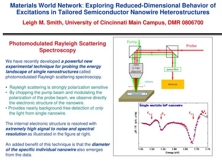
Materials World Network: Exploring Reduced-Dimensional Behavior of Excitations in Tailored Semiconductor NanowireHeterostructuresLeigh M. Smith, University of Cincinnati Main Campus, DMR 0806700 • Photomodulated Rayleigh Scattering Spectroscopy • We have recently developed a powerful new experimental technique for probing the energy landscape of single nanostructures called photomodulated Rayleigh scattering spectroscopy. • Rayleigh scattering is strongly polarization sensitive • By chopping the pump beam and modulating the • polarization of the probe beam, we observe directly • the electronic structure of the nanowire. • Provides nearly background-free detection of only • the light from single nanowire. • The internal electronic structure is resolved with • extremely high signal to noise and spectral • resolution as illustrated in the figure at right. • An added benefit of this technique is that the diameter • of the specific individual nanowire also emerges • from the data.
Materials World Network: Exploring Reduced-Dimensional Behavior of Excitations in Tailored Semiconductor NanowireHeterostructuresLeigh M. Smith, University of Cincinnati Main Campus, DMR 0806700 • Broader Impact Highlights • Nano-based Educational Activities • (at both U. Cinn. & Miami U.) • – Reached a total of approx. 1170 young people since 2008 • 3 Sophomore-based science lecture, lab & computational undergraduate • courses - 90 students each year • “Physics & Society” nonscience course – 140 undergraduates each semester • High School Chemistry & Physics Classes – 172 students annually • Nanoscience & Technology Outreach Programs • Reached 2 high school teachers, 240 5th & 8th graders, and 237 in other programs since 2008 5th Graders, 8th Graders, & Nonscience Undergraduates All learning “What’s nano?”