Download
1 / 22
220 likes | 222 Views
This project aims to develop a switching nano-crossbar computer using four-terminal switches and optimize its performance. The project is funded by the European Union and supported by TUBITAK-Career project.

E N D
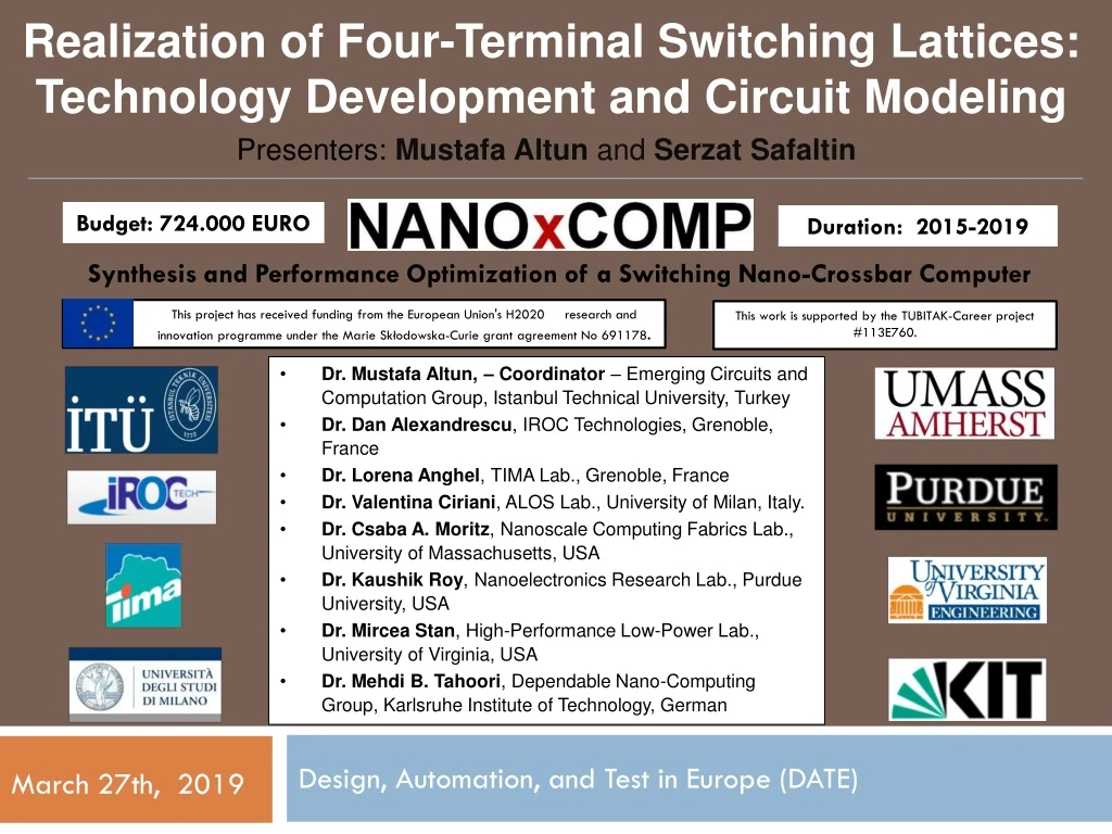
Presenters: Mustafa Altun andSerzatSafaltin Budget: 724.000 EURO Duration: 2015-2019 Synthesis and Performance Optimization of a Switching Nano-Crossbar Computer This project has received funding from the European Union's H2020 research and innovation programmeunder the Marie Skłodowska-Curie grant agreement No 691178. This work is supported by the TUBITAK-Career project #113E760. • Dr. Mustafa Altun, – Coordinator – Emerging Circuits and Computation Group, Istanbul Technical University, Turkey • Dr. Dan Alexandrescu, IROC Technologies, Grenoble, France • Dr. Lorena Anghel, TIMA Lab., Grenoble, France • Dr. Valentina Ciriani, ALOS Lab., University of Milan, Italy. • Dr. Csaba A. Moritz, Nanoscale Computing Fabrics Lab., University of Massachusetts, USA • Dr. Kaushik Roy, Nanoelectronics Research Lab., Purdue University, USA • Dr. Mircea Stan, High-Performance Low-Power Lab., University of Virginia, USA • Dr. Mehdi B. Tahoori, Dependable Nano-Computing Group, Karlsruhe Institute of Technology, German Realization of Four-Terminal Switching Lattices: Technology Development and Circuit Modeling Design, Automation, and Test in Europe (DATE) March 27th, 2019
Project Flow • Why weusefour-terminal switches? • How torealizethem? • Whichtechnology?
Two-terminal vs. Four-terminal • The Boolean functions implemented in (a) ad (b)aresame!
Logic Synthesis Problem How can we implement a given target Boolean function fTwith a lattice of four-terminal switches? Example:fT= x1x2x3+x1x4
Logic Synthesis Problem Example:fT= x1x2x3+x1x4+x1x5 9 TOP-TO-BOTTOM PATHS!
First Method’s Performance fT= x1x2x3+x1x4+x1x5 fTD= x1 + x2x4x5 + x3x4x5 Size of the lattice:m×n nandmare the number of products of the target functionfTand its dual fTD, respectively.
OtherSynthesis Methods • Optimal andheuristicsmethodstodecreaselattice size • Methodsbased on SAT • Methodsbased on decompositions • Methodsforspesifictype of funtionssuch as parityfunctions • Methodsusingmulti-lattices • Methodsformulti-outputfunctions • Switchinglattices has a greatcomputingpotential
Computing Potential • Switchinglattices has a greatcomputingpotential
TechnologyforSwitchingLattices • How aboutthetechnology? • WeproposeCMOS-compatibletechnologywith TCAD simulations • By fitting the TCAD datato the standard CMOS current-voltage equations, we develop aSpice model of a four-terminal switch • Wearecurrentlyworkingtowardthefabrication.
Device Structures • 1: Diffusion region 2: Gate electrode 3. Gate insulator region • 4: Local Oxidation of Silicon (LOCOS) or Shallow Trench Isolation (STI) layers • 5: Bulk layer
Device Structures • 1: Diffusion region 2: Gate electrode 3. Gate insulator region • 4: Local Oxidation of Silicon (LOCOS) or Shallow Trench Isolation (STI) layers • 5: Bulk layer
Device Structures • 1: Diffusion region 2: Gate electrode 3. Gate insulator region • 4: Local Oxidation of Silicon (LOCOS) or Shallow Trench Isolation (STI) layers • 5: Bulk layer
FabricationSteps • Challengesforintegration of 4-terminal architecture • 2D – compatiblewithcurrent and emergingfabricationmethods... • 3D – wiring and criticaldimensionlimitsoperationbut greatpotentialfor dense wiring… • Materials? • same as 2-terminal devices • Four-TerminalLogicRealization • Structure? • GAA, VGAA, M3D, finegrainedvertical 3D, FinFET… • Device Type? • Depletion, Immersion • Whatworksfor 2-terminal approachwillworkfor4-terminal.
FabricationSteps • Device scaling • compatible to state-of-art (Moore’sLaw) • TCAD vsExperimental Device • leakagecurrent • isolationlimits • What can be done with 2-terminal device can also be done with 4-terminal deviceapproach.
FabricationSteps T4 T2 • Fabrication Plan 1 • First plan is to fabricatejunctionlessdevice… • Pros: no doping steps. • Cons: scaledependent, low ON/OFF ratio. • SOI substrate, simpleprocessflow… • 2-terminal fabricationprocesses can be implementedwithminormodification… T1 T3
FabricationSteps • EBL RIE EBL ALD EBL Metallization StartingWafer Material: SOI Si, N-type RIE E-BeamLithography RIE
FabricationSteps E-BeamLithography AtomicLayerDeposition Lift-off Metal deposition
FabricationSteps • Fabrication Plan 2 • Squareshaped N-typeor P-type MOSFET • Pros: pnjunction, high ON/OFF ratio. • Cons: scaling-doping-geometricfeatures… • At least 20 processstepsincludinglithography, deposition, etching, surfacecleaning… T4 T2 T1 T3
FabricationSteps • Future • novelmaterials • SiGe, high-k gateoxides… • 2D materials • graphene, MoS2… • FlexibleCircuits • metal-organic network, conductivepolymers • NovelFabricationMethods • nanoinkjetprinting, nanoimprintlithography, selective EPI growth… • Advancement of 2-terminal devices and systemshavesame trend with 4-terminal devices
EmergingCircuitsandComputationGroup • Web: http://www.ecc.itu.edu.tr/ THANK YOU!