Download
1 / 1
10 likes | 233 Views
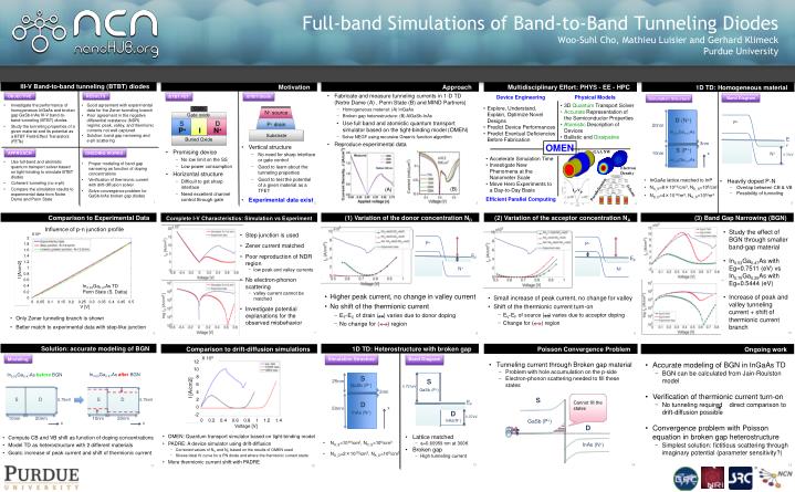
Full-band Simulations of Band-to-Band Tunneling Diodes Woo-Suhl Cho, Mathieu Luisier and Gerhard Klimeck Purdue University. III-V Band-to-band tunneling (BTBT) diodes. Comparison to drift-diffusion simulations. Solution: accurate modeling of BGN. Comparison to Experimental Data.

E N D
Full-band Simulations of Band-to-Band Tunneling DiodesWoo-Suhl Cho, Mathieu Luisier and Gerhard KlimeckPurdue University III-V Band-to-band tunneling (BTBT) diodes Comparison to drift-diffusion simulations Solution: accurate modeling of BGN Comparison to Experimental Data 1D TD: Heterostructure with broken gap Multidisciplinary Effort: PHYS - EE - HPC (2) Variation of the acceptor concentration NA Approach Ongoing work (3) Band Gap Narrowing (BGN) (1) Variation of the donor concentration ND 1D TD: Homogeneous material Complete I-V Characteristics: Simulation vs Experiment • Investigate the performance of homogeneous InGaAs and broken gap GaSb-InAs III-V band-to-band-tunneling (BTBT) diodes • Study the tunneling properties of a given material and its potential as a BTBT Field-Effect Transistors (FETs) • Use full-band and atomistic quantum transport solver based on tight-binding to simulate BTBT diodes • Coherent tunneling (no e-ph) • Compare the simulation results to experimental data from Notre Dame and Penn State • Fabricate and measure tunneling currents in 1-D TD (Notre Dame (A) , Penn State (B) and MIND Partners) • Homogeneous material: (A) InGaAs • Broken gap heterostructure: (B) AlGaSb-InAs • Use full band and atomistic quantum transport simulator based on the tight-binding model (OMEN) • Solve NEGF using recursive Green’s function algorithm • Reproduce experimental data X106 X 105 Device Engineering Physical Models Simulation Structure RESULTS Band Diagram OBJECTIVE Modeling Band Diagram Influence of p-n junction profile Simulation Structure 12 10 8 6 4 2 0 -2 2 1.8 1.6 1.4 1.2 1 0.8 0.6 0.4 0.2 0 • Good agreement with experimental data for the Zener tunneling branch • Poor agreement in the negative differential resistance (NDR) regime: peak, valley, and thermionic currents not well captured • Solution: band gap narrowing and e-ph scattering • Proper modeling of band gap narrowing as function of doping concentrations • Verification of thermionic current with drift-diffusion solver • Solve convergence problem for GaSb-InAs broken gap diodes • Accurate modeling of BGN in InGaAs TD • BGN can be calculated from Jain-Roulston model • Verification of thermionic current turn-on • No tunneling required direct comparison to drift-diffusion possible • Convergence problem with Poisson equation in broken gap heterostructure • Simplest solution: fictitious scattering through imaginary potential (parameter sensitivity?) • Study the effect of BGN through smaller band-gap material • In0.53Ga0.47As with Eg=0.7511 (eV) vs In0.75Ga0.25As with Eg=0.5444 (eV) • Increase of peak and valley tunneling current + shift of thermionic current branch • Step junction is used • Zener current matched • Poor reproduction of NDR region • low peak and valley currents • No electron-phonon scattering • valley current cannot be matched • Investigate potential explanations for the observed misbehavior • 3D Quantum Transport Solver • Accurate Representation of the Semiconductor Properties • Atomistic Description of Devices • Ballistic and Dissipative In0.53Ga0.47As after BGN • Explore, Understand, Explain, Optimize Novel Designs • Predict Device Performances • Predict Eventual Deficiencies Before Fabrication In0.53Ga0.47As before BGN Gate 3nm S 2nm Gate oxide I [A/cm2] P+ P+ P+ S S D D N+ source GaSb (P+) S D S D 0.751eV D (N+) S (P+) I [A/cm2] 0.75eV 0.75eV EF EF P+ I N+ x x GaSb (P+) S InAs (N+) x EF In0.53Ga0.47As GAA NW 20nm 20nm P+ drain 10nm 10nm OMEN EF Cannot fill the states x 0.75eV D In0.53Ga0.47As Substrate Buried Oxide ONGOING WORKS APPROACH Motivation • Accelerate Simulation Time • Investigate New Phenomena at the Nanometer Scale • Move Hero Experiments to a Day-to-Day Basis N+ N+ N+ Electron Density In0.53Ga0.47As TD Penn State (S. Datta) GaSb (P+) 0.37eV 50nm 25nm InAs(N+) 0 0.2 0.4 0.6 0.8 1 1.2 1.4 Voltage [V] BTBT Diode BTBT FET D 10nm 20nm • Higher peak current, no change in valley current • No shift of the thermionic current • EF-EC of drain ( ) varies due to donor doping • No change for ( ) region • Small increase of peak current, no change for valley • Shift of the thermionic current turn-on • EV-EF of source ( ) varies due to acceptor doping • Change for ( ) region 0 0.05 0.1 0.15 0.2 0.25 0.3 0.35 0.4 0.45 0.5 V [V] e e • Lattice matched • a=0.60959 nm at 300K • Broken gap • High tunneling current • InGaAs lattice matched to InP • NA_S=8×10¹⁹/cm3, ND_S=106/cm3 • ND_D=4×10¹⁹/m3, NA_D=106/m3 • Heavily doped P-N • Overlap between CB & VB • Possibility of tunneling • OMEN: Quantum transport simulator based on tight-binding model • PADRE: A device simulator using drift-diffusion • Corrected values of NV and NC based on the results of OMEN used • Shows ideal IV curve for a PN diode and where the thermionic current starts • More thermionic current shift with PADRE • Compute CB and VB shift as function of doping concentrations • Model TD as heterostructure with 2 different materials • Goals: increase of peak current and shift of thermionic current Parallelization • NA_S=1019/cm3, ND_S=106/cm3 • ND_D=2×10¹⁸/cm3, NA_D=106/cm3 Id-Vgs Scheme InAs (N+) (B) (A) • Only Zener tunneling branch is shown • Better match to experimental data with step-like junction 15 Efficient Parallel Computing 5 13 4 11 10 12 9 7 8 6 • Promising device • No low limit on the SS • Low power consumption • Horizontal structure • Difficult to get sharp interface • Need excellent channel control through gate • Vertical structure • No need for sharp interface or gate control • Good to learn about the tunneling properties • Good to test the potential of a given material as a TFET • Experimental data exist 1 2 3 Poisson Convergence Problem • Tunneling current through Broken gap material • Problem with hole accumulation on the p-side • Electron-phonon scattering needed to fill these states 14