Download

1 / 8
80 likes | 205 Views
Status report of Resistive Strips Preparation. Atsuhiko Ochi, Kobe University. 16/04/2014 MM PCB WG mtg @ CERN. Large size resistive strip production. 2013 October First trial to make a large size sample 870mm x 425mm trapezoidal shape 8 foils are produced

E N D
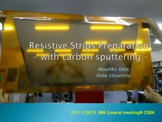
Status report of Resistive Strips Preparation AtsuhikoOchi, Kobe University 16/04/2014 MM PCB WG mtg@ CERN
Large size resistive strip production • 2013 October • First trial to make a large size sample • 870mm x 425mm trapezoidal shape • 8 foils are produced • Provided as a MSW resistive strips • 2014 March • Second trial • Same size as first trial • 3foils are produced • 2014 April • Third trial • 50cm x 40cm rectangle shape • 2 foils are produced • Provided as a new test chamber A. Ochi, MM PCB WG
Micro scorpic pictures of strips • Recent rectangle foil • Strip width: 0.35mm • Gap width: 0.1mm • Foils are attached on PET film • To avoid the damage of the sputtered carbon pattern, by bending the foil Sputtered pattern 50 μm polyimide foil PET FILM A. Ochi, MM PCB WG
Resistivity check • Resistivity from HV source bar • Line resistivity : 15MΩ/cm • Carbon sputter thickness: 310 nm Y x Preliminary Surface Resistivity [MΩ/sq.] Cupper thickness [Ǻ] A. Ochi, MM PCB WG
Problem in liftoff process On the liftoff process • It is not easy to remove the wide resist pattern (correspond to non resistive pattern) • Long exposure in NaOH liquid may cause the damage to sputtered patterns • This is more critical for outside of the pattern • Currently, we have masked outside area by tape and other sheet by hand • However, it is time and cost consuming NaOH Sputtered carbon resist Substrate (polyimide) Sputtered carbon Substrate (polyimide) A. Ochi, MM PCB WG
Request for new pattern- Dummy resistive coating - • Can we put dummy resistive coating around the resistive strip pattern with < 5mm gap? • Do we have to consider the mesh attachment and O-ring attachment ? Resistive strip pattern Dummy resistive coating A. Ochi, MM PCB WG
Feasibility for Module-0 • Technical challenging • There are more than 2m long foils! • 16 types 64 foils needed • Are there resistivity variability for different sputtering batch ? • It should be checked. • Fast sputtering method should be developed for reducing the cost. • Currently: 6 hours/batch • Next trial: 2.5hours/batch, using multiple sputtering target • Shorter time available ? A. Ochi, MM PCB WG
Summary and prospects • Currently, resistive foils production using sputtering is succeeded for large foils. • To reduce the process and the cost, dummy sputtering is needed. • 2.2m long foils can be made! • Discussion of the cost should be started. A. Ochi, MM PCB WG