Download
1 / 40
410 likes | 687 Views
Thin-film Solar Cells Friday 07:00-09:00 pm Textbook: Solar Cells edited by T. Markvart and L. Castaner Lecturer: Prof. Yeong-Cheol Kim. Chap. Iic-1 Amorphous silicon solar cells Introduction Amorphous silicon alloys Deposition conditions and microstructure Optoelectronic properties

E N D
Thin-film Solar Cells Friday 07:00-09:00 pm Textbook: Solar Cells edited by T. Markvart and L. Castaner Lecturer: Prof. Yeong-Cheol Kim
Chap. Iic-1 Amorphous silicon solar cells • Introduction • Amorphous silicon alloys • Deposition conditions and microstructure • Optoelectronic properties • Doping • Light-induced degradation • Amorphous silicon solar cells • Physics of operation • Device structures • Performance and stability • Reliability • Production of amorphous silicon solar cells • Manufacturing process • Manufacturing costs • Environmental issues • Future trends
Introduction • - large-area deposition techniques for mass production • - 40 organizations • - first investigation, silane discharge, Chittik, 1969. • - lower density of defects than evaporated or sputtered a-Si. • - doping by Carlson, Spear&LeComber • - Carlson&Wronski, efficiency 2% in 1976. • - 5% • - H, alloy of H and Si, hydrogenated a-Si (a-Si:H). • - Staebler-Wronski effect (SWE): large change in photoconductivity, reversible at 150C for a few hrs. • - how to minimize the effect.
- PECVD, DC, RF, VHF (30~110 MHz), microwave (~2.45 GHz) - substrate T: ~200-250C - dilution of silane with hydrogen, protocrystalline a-Si:H - bandgap change by H. - C or Ge - wide bandgap p-type a-Si:C:H alloys: little absorption, high built-in potentials. - narrow bandgap a-Si:Ge:H: tandem and triple junction cells. - C or Ge alloying: additional defect states - ~1.3 eV (~75 at.% Ge) to ~2.1 eV (~15 at.% C) - multijunction allows thinner component cells, reduce SWE. - decrease in absorption of sunlight, increase in shorts and shunts. - optical inhancement by textured optical reflectors. - PECVD, excellent uniformity over 1 m2 area. - RCA lab.: curing of shorts and shunts by reverse bias, laser scribing process, large-area, monolithic PV module of a-Si SCs connected in series.
2. Amorphous silicon alloys 2.1 Deposition conditions and microstructure - decomposition of feedstock gases by plasmas, DC, RF (13.56 MHz), VHF (30-110 MHz), microwave (2.45 GHz). - SiH4 decomposed by e impact into mixture of radical and ionic species. - variables: sub T, P, flow rate, plasma power, frequency, electrode spacing, source gases. - impurities, O, C, N - T, reactions on surface material quality - P, mean free path for collision reaction locations - flow rate, residence time growth kinetics - power, rate of dissociation film growth rate - frequency, nature of plasma ion bombardment, less significant at VHF and micro. - GeH4, CH4, dopant gases. - H, key element - variables, interdependent complex PECVD process
2. Amorphous silicon alloys 2.1 Deposition conditions and microstructure - deposition process dissociation of molecules transport to surface by diffusion reaction desorption of byproducts and unreacted silane radicals. optimum condition: pure silane or H-diluted silane, low RF power, 200-300C substrate T - H in plasma, passivate dangling bonds, reconstruction of network. - H dilution, R=[H2]/[SiH4]=10, thickness dependent microstructure. - initially amorphous, eventually microcrystalline
2. Amorphous silicon alloys 2.1 Deposition conditions and microstructure - rapid decrease of proto regime at high H dilutions limit i-layer thickness - H increases bandgap. Figure 1. Film thickness at which the different phase transitions occur during Si:H film growth plotted as a function of the hydrogen dilution ratio R.
2. Amorphous silicon alloys 2.2 Optoelectronic properties - absence of long-range order bandtails, localized states due to disorder, broken bonds. - carrier trapping, recombination centers. - high absorption coefficient due to random nature of atomic ordering. - H incorporation, reduce defects, widen gap. - densities of dangling bonds < 1016 cm-3 inPECVD a-Si:H with H~10 at.%.
2. Amorphous silicon alloys 2.3 Doping - undoped, slightly n-type - dopant introduction, move EF towards conduction and valence band. - high density dopants, defect states at midgap limit doping efficiency, lifetime. - doped materials are not appropriate for absorber layers. - thin films of p-type a-SiC:H or protocrystalline Si:H for p/i heterojunctions. - n-type a-SiC:H and uc-Si:H as ohmic contacts. - p-i-n or n-i-p cells
2. Amorphous silicon alloys 2.4 Light-induced degradation - SWE - no general consensus on exact nature of light-induced defects. - because of no unique a-Si:H material. - neutral dangling bonds, charged defects
3. Amorphous silicon solar cells 3.1 Physics of operation - p-i-n or n-i-p heterojunction cell structure
3. Amorphous silicon solar cells 3.1 Physics of operation - choice of TCO materials (window layer), optical transmission, conductivities, good contact to p-layers. - p-type: ~10 nm - carriers collected by inter electric field, drift current. - adverse effect of defects: recombination centers, reduce E field. - buffer layer in p/i later
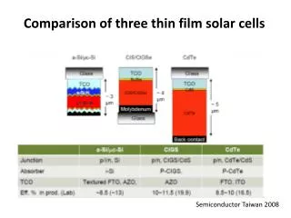
3. Amorphous silicon solar cells 3.2 Device structures - multijunction structures, higher stabilized efficiencies - substrates: float glass, BP Solar, Energy Photovoltaics, Intersolar, Kaneka, Phototronics, Sanyo, Sharp SS, Canon, United Solar Systems plastic substrates, Fuji Electric, Iowa Thin Films, Sanyo - glass/textured tin oxide/p-i1-n/p-i2-n/zinc oxide/Al/EVA/glass, BP Solar i1, A-Si:H, i2, a-SiGe:H - SS foil/textured silver/zinc oxide/n-i3-p/n-i2-p/n-i1-p/ITO/EVA/fluoropolymer i2, i3, a-SiGe:H, i1, a-Si:H fluoropolymer, Tefzel by DuPont roll-to-roll, multi-chamber PECVD system
3. Amorphous silicon solar cells 3.3 Performance and stability - light-induced degradation, triple-junction, 10-15%
3. Amorphous silicon solar cells 3.4 Reliability - electrical performance, electrical isolation (dry and wet), visual inspection, thermal cycling between -40 and +85 C, light soaking, ultraviolet light exposure, humidity freeze cycling between -40 and +85 C (85% humidity above room T.), static and dynamic mechanical loading, hail impact tests, surface cut susceptibility, hot-spot endurance and outdoor exposure. - moisture ingression, delamination for thin-film SC.
4. Production of amorphous silicon solar cells BP Solar, tandem modules on glass United Solar, triple-junction modules on SS foil Iowa Thin Films, single-junction modules on plastic 4.1 Manufacturing process - a-Si/a-SiGe tandem modules - ~9 mm wide scribing by Nd:YAG laser - ~15 um in diameter
Plasma frequency 1 Reflectivity ω→ 0 wp Angular Frequency
4. Production of amorphous silicon solar cells 4.2 Manufacturing costs - BIPV: roofing shingles, PV laminates by Uni-Solar, PowerView by BP Solar
4. Production of amorphous silicon solar cells 4.3 Environmental issues - mining and refining raw materials, manufacturing PV modules, disposing obsolete modules. - trimethylboron (~1-5% in silane), less toxic than diborane. - silane, pyrophoric. - no wet chemicals in BP - no harmful materials in PV modules, breakage, fires, or long-term disposal in landfills.
5. Future trends - Sanyo in 1980 for calculators, 3.5 MWp by 1985 - ~40 MWp in 2001. - key drivers for terrestrial PV market: efficiency, price, reliability. - balance of system, area-related costs. - stabilized efficiency, lower manufacturing cost, long term reliability - microcrystalline Si - BIPV
Industry status Oerlikon solar : better (and cheaper) reflective backsheet, thinner silicon layer Pramac: 9.2% Sharp, IBC solar: 10% Schott ASI TM 103: 7.1% Kaneka GSA-60: 6.3% Inventux X 140: 9.8% Uni-Solar PVL-144: 6.7%
Oerlikon Solar ThinFab production line Micromorph tandem 1.4m2 solar module 10% 143Wp EUR 0.5/Wp
Solar cell panel price ($1/Wp) vs. 1 kWh price System price: $2.5/Wp Electric power of 1W cell: 1Wx3.5hrx365daysx20year=25.5kWh Therefore, $2.5/25.5kWh=$0.1/kWh