Download
1 / 38
380 likes | 525 Views
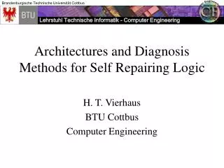
Architectures and Diagnosis Methods for Self Repairing Logic. H. T. Vierhaus BTU Cottbus Computer Engineering. Outline. 1. Parameters for Self Repair Functions. 2. Self Repair Based on FPGAs. 3. PLAs and CPLDs. 4. Duplication and Switched Logic Blocks.

E N D
Architectures and Diagnosis Methods for Self Repairing Logic H. T. Vierhaus BTU Cottbus Computer Engineering
Outline 1. Parameters for Self Repair Functions 2. Self Repair Based on FPGAs 3. PLAs and CPLDs 4. Duplication and Switched Logic Blocks 5. Fault Diagnosis and Fault Administration 6. Test and Fault Diagnosis 7. Some Parameters in Comparison 8. Summary and Conclusions
Basic Parameters for BISR Fault densities that can be managed Types of faults that can / cannot be repaired Overhead (chip area, time, dissipated power) Compatibility with standard CMOS processes Applicability to BISR in a production - test environment or in the field of application
Repair Granularity and Fault Density Block- Ersatz (ALU etc.) Makro-Ersatz (CPU etc.) Hardly Logic / Gate Level Ersatz explored (logic) Expected fault density (1 out of..) CPU RT- macro FPGA trans. trans. gate gate cores block 10 10 10 10 10 10 10 10 10 10 10 10 10 10 Granularity Granularity 0 0 1 1 2 2 3 3 4 4 5 5 6 6 (transistors) (transistors)
Repair Overhead versus Element Loss Repair procedure Functioning overhead elements lost New Methods and Archi- techtures Prohibitive overhead Prohibitive fault density 10 1k 10k 100k 1M 10M 1 100 Size of replaced blocks (granularity)
Block Structure of FPGAs Programmable interconnects
FPGA Experiences FPGA repair schemes that discard a whole row or column of CLBs are simple to implement but inefficient, as they lose many functional CLBs for a single fault. FPGA schemes that reserve single CLBs in the matrix for backup and do repair by single CLB replacement are much more difficult to implement because of the necessary irregular-wiring process.
FPGA with Irregular Repair Scheme Programmable interconnects CLB CLB CLB CLB functionally used CLBs CLB CLB CLB CLB Backup block used for replacement row with CLB CLB CLB CLB faulty CLB used CLB CLB CLB CLB CLBs CLB CLB CLB CLB backup block (reserved)
BISR by Standard FPGAs ? Configurable logic blocks (CLBs) are rather large (5000-10 000 transistors, estimated) • FPGAs are heterogeneous by nature: • memory-like lookup tables • logic elements (selectors, decoders, flip-flops, • embedded arithmetic units) • local and global programmable interconnects with • additional elements for programmability • - embedded CPUs. For fault densities below about 1 in 10 000, repair must go into CLBs or slices !
Self Repair within FPGA Basic Blocks Heterogeneous repair strategies required (memory, logic) Logic blocks may use methods known from memory BISR Additional repair strategies are necesssary for logic elements The basic overhead for FPGAs versus standard logic (about 10) is enhanced. Repair strategies for logic may use some features already used in FPGAs (e. g. switched interconnects).
PLA Repair Scheme Switching unit Switching Unit Specific programming of cross points !
FPGA / CPLD Repair Looks pretty easy at first glance because of regular architecture Requires lines / colums of switches for configuration at inputs and between AND / OR matrices Requires additional programmability of cross-points by double-gate transistor as in EEPROMs or Flash memory Not fully compatible with standard CMOS Limited number of (re-) configurations Floating gate (FAMOS) transistors are fault-sensitive !
Cell Duplicaton Simple scheme involving VDD off / on switch Inherent duplication of efforts VDD separation of fault cells Extra effort for output isolation of fault cells necessary. Input isolation (input gate shorts) is not easily possible. Relatively large overhead for managing repair states and redundance (re-) organisation. Fully CMOS compatible
Logic Cluster Architecture A number of equal-type logic gates makes a cluster The cluster contains one or more spare gates A spare gate may replace a normal device, modification is done via sets of input / output selctors / de-selectors Problems: Input gate short of a „normal“ device is not fully isolated For n gates alternatively mapped to a single backup device, there are (n+1) control states. Switching elements are complex and not fault tolerant By themselves.
Modified Cluster Architecture Can possibly isolate a specific gate, but still requires lots of administrative overhead.
Reconfiguration by Permutation Schemes 2-Way Switch state 0 grounded „faulty“ inputs / outputs state 1
Specific Features Only 4 logic states for permutation in a cluster of 8 logic blocks including 2 for backup. All single failed blocks plus some double failures can be compensated. Failed components are isolated and input / output grounded. Input gate shorts can be handled. Internal blocks may have different complexities depending on anticipated fault density. Simple switching devices, fully CMOS compatible. Fault tolerant switching devices need extra effort !
Fault Tolerant Switch s s in out s s Switching elements can be made fault-tolerant by themselves, both for on- and off-type faults ! ... but at the cost of extra delays !
Test, Diagnosis, Fault Administration For self rapair in the field of application, fault diagnosis must identify faulty elements that can be replaced. The granularity of fault diagnosis is therefore depending on the granularity of replacement (gates, RT-elements, CPUs) Conventional fault diagnosis in scan-based test is limited to the respective position in a scan chain. As scan chains are often allocated in a random manner without a strict reference to RT-level architectures, diagnosis methods used with production test are not a real solution. • A system that has redundant elements and self-repair functions must • restore a „working“ status after power-off periods by: • storage and re-assembly of the previous status of repair, or by • - self test, fault diagnosis and re-configuration after start-up.
Test and Redundancy Administration Status control System With BISR Capability CPU Repair Status Memory Redundant Elements ... makes a significant overhead beyond redundancy provision !
Test and Diagnostic Resolution (1) Scan - in G1 G2 G3 G4 G5 G6 G7 G8 G9 G10 G11 G12 G13 Scan - out Scan test can only identify faulty scan-out location !
Test and Diagnostic Resolution (2) Scan - in G1 G2 G3 G4 G5 G6 Non-resolvable fault ! G7 G8 G9 G10 G11 G12 G13 Scan - out Scan test can only identify faulty scan-out location ! Further resolution by multiple test patterns !
Production Test with Diagnosis Test Fault Detection Scan-Path Nr., Bit-Nr. Diagnosis On-line Off-line Fault simulation Layout .. is not available in the field ! Chip-Analysis
Tentative Repair Switch-off of faulty elements and power separation are often done by „fuses“. Once a fuse is blown, it cannot be re-installed !! Reconfiguration schemes based on „fuse“ or „antifuse“ switching elements cannot be used in conjunction with „tentative repair“.
Enhanced Logic Cluster Extra scan outs at extra blocks
Diagnostic Test In a bundle of 8 blocks and with 2 extra outputs. By going through the 4 logic states of (re-)configuration, each block is once connected to the „spare“ inputs and outputs. If a test pattern is applied to 4 units of the same type by going through the 4 states, the faulty unit can be identified. The „false“ output detection can be used locally to set a status of re-configuration. With multiple units of the same type tested in parallel, time and overhead are resonable. If tests are short and reliable, an initial test process after every power-down can be performed. Keeping configurations in a memory is not necessary.
Integrated Test & Repair logic R logic R Global Control BIST&Repair BIST&Repair BIST start logic R logic R BIST&Repair BIST&Repair Monitoring of „repair resources exhausted“ conditions logic R logic R BIST&Repair BIST&Repair
Summary Several types of logic (FPGAs, CPLDs) require either an inhomogeneous replacement process based on different types of redundant elements. Repair schems that need special devices (e. g. floating gate transistors) are not attractive. Schemes that provide a high level of fault isolation for short-type faults are most attractive. Architectures that also provide excellent local (self-) test coupled to locally organized self repair are possible.