Download
1 / 27
290 likes | 481 Views
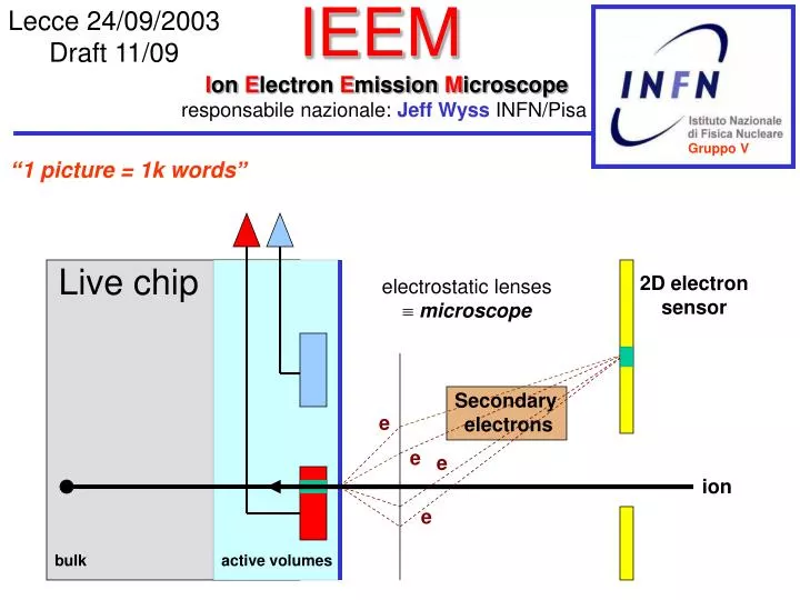
Lecce 24/09/2003 Draft 11/09. responsabile nazionale: Jeff Wyss INFN/Pisa. IEEM. Gruppo V. “1 picture = 1k words”. Live chip. 2D electron sensor. electrostatic lenses microscope. I on E lectron E mission M icroscope. Secondary electrons. e. e. e. ion. e. bulk.

E N D
Lecce 24/09/2003 Draft 11/09 responsabile nazionale: Jeff Wyss INFN/Pisa IEEM Gruppo V “1 picture = 1k words” Live chip 2D electron sensor electrostatic lenses microscope Ion Electron Emission Microscope Secondary electrons e e e ion e bulk active volumes
IEEMMicroscopio ASSIALE ad emissione di elettroni per impatto ionico • Sezioni INFN: Pisa, Padova, Roma2 • Linea di ricerca: Single Event Effects (SEE) indotti da ioni energetici in dispositivi e sistemi microelettronici per applicazioni spaziali, di fisica delle alte energie, ed industriali. • Laboratorio e facility: Legnaro, Tandem XTU da 15MV, linea di irraggiamento con ioni SIRAD (Li-Au). • Processo fisico: correlazione su scala micrometrica tra i punti di impatto ionico e SEE indotti in vari dispositivi (ASIC, commerciali, strutture di test) mediante l’uso di un microscopio assialead emissione di elettroni secondari da impatto ionico normale. • Durata e preventivo globale:due anni, 130 kEuro • 2004:costruzione, installazione IEEM con sistema di test SDRAM sulla linea SIRAD, risultati preliminari; • Preventivo 2004 (kEuro):25 (PI) + 48 (PD) + 20 (RM2) = 93 • 2005:messa a punto e presa dati.
What is SIRAD SIRADis the acronym forSIlicon andRADiation. The purpose of the SIRAD facility is: "investigate radiation effects on silicon detectors, micro-electronic devices and systems in radiation hostile environments". - Total Dose Effects: cumulative effects due to ionization (dose). - Bulk Effects: cumulative effects due to displacement damage (fluence). - Single Event Effects: instantaneous effects resulting from the strike of a single energetic particle (probability, cross-section). - High Energy Physics experiments (CDF, CMS,...). - Space missions of scientific satellites (GLAST, AGILE, PAMELA,...) • silicon detectors (CDF, CMS, SMART) • ASIC microelectronics (CMS, GLAST, AGILE) • commercial off the shelf microelectronics (FPGA, FLASH, SDRAM, power devices) • test structures (physics of ultra-thin oxide rupture)
The SIRAD beam line (protons and ions) Accelerator: - Tandem Van de Graaff; - 15 MV maximum voltage; - two strippers. ions from H (30 MeV) to Au (300 MeV) NOTE: The AXIAL IEEM will be installed downstream of SIRAD chamber to COEXIST with the intense and successful SIRAD program.
Ion beams available at SIRAD •Ion species from1H (23-30 MeV) up to197Au (1.4 MeV/a.m.u.) • LET from 0.02 MeVcm2/mg(1H) up to 81.7 MeVcm2/mg (197Au)
Institutions and industrial partners participating to SIRAD The experiments are performed in collaboration with more than80 scientists and researchers from 26 Italian and foreign institutions and industrial partners [1] INFN, Laboratori Nazionali di Legnaro [2] INFN, Sezione di Padova [3] INFN, Sezione di Perugia [4] INFN, Sezione di Pisa [5] INFN, Sezione di Trieste [6] Dipartimento di Fisica, Università di Padova [7] Dipartimento di Fisica, Università di Perugia [8] Dipartimento di Fisica, Università di Trieste [9] Dipartimento di Automatica e Informatica, Politecnico di Torino [10] Dipartimento di Elettronica ed Informatica, Università di Padova [11] Dipartimento di Ingegneria, Università di Ferrara [12] Dipartimento di Meccanica, Struttura, Ambiente e Territorio, Università di Cassino [13] Istituto di Astrofisica Spaziale e Fisica Cosmica (IASF), Sezione di Roma. [14] Istituto di Astrofisicia Spaziale e Fisica Cosmica (IASF), Sezione di Bologna [15] Dipartimento di Ingegneria Elettronica, Università Autonoma di Barcellona, Spagna [16] ENSERG-INPG, Grenoble (France) [17] GSI, Darmstadt (Germany) [18]Institut de Microelectrònica de Barcelona (IMB), CNM-CSIC, Barcelona, Spain [19] Lawrence Berkeley National Laboratory (LBL), Berkeley, USA [20] LETI-CEA, Grenoble (France) [21] Institute of Physics, Academia Sinica, Taiwan [22] SCIPP-University of California at Santa Cruz (UCSC), Santa Cruz, USA [23] Aurelia Microelettronica, Navacchio Cascina (PI) [24] Center for Advanced Research in Space Optics (CARSO), Area Science Park, Trieste [25] Istituto di Ricerca Trentino (IRST), Trento [26] ST Microelectronics, Agrate Brianza (MI) INFN A SIRAD 5 anni di attivita` piu` di 30 pubblicazioni nel 2002-2003 (IEEE, NIM A ann B, Microelectronics Reliability, conferenze NREC, RADCES, ICNMTA IBA,...). Circa 15 articoli sottomessi nel 2003.
Beam time allocation at SIRAD in 2002 (26 days) Single Event Effects: 71% An IEEM would be COOL!
Single Event Effects (SEE) A single incident particle may produce directly or indirectly enough energy in the form of ionization to cause asingle macroscopic(anomalous) effect in a polarized device. e.g. or NEUTRON A nuclear spallation reaction induced by protons and neutrons. Top: cascade stage in which fast secondaries emerge in the forward direction. Middle: evaporation stage in which secondary protons, neutrons, deuterons and alphas particles emerge isotropically. Bottom: recoil stage in which the residual fragment of the target nucleus emerges with the momentum gained in the earlier stage. SEEeffects are induced in a live electronic device if the ionization induced in the sensitive volume of the device by a primary ionizing particle orby secondary particles or by a recoiling nucleus is higher than some characteristic SEE threshold value.
SEE-OLOGY For a given radiation environment (HEP experimental hall, orbit in outer space mission, solar activity) the mechanisms of an SEE and the PROBABILITY of it occurring aredevice and technology dependent. -destructive events: Single Event Burnout (SEB) in power DMOS transistor Single Event Snapback (SES) in MOSFET Single Event Gate Rupture (SEGR) in DMOS transistor Single Event Latch-up (SEL) in CMOS technologies -non destructive events: Single Event Drain Current Collapse (SEDC2) Single Event Upset (SEU) Single Event Disturb (SED) Single Event Transient (SET) Single Event Functional Interrupt (SEFI)
Radiation Effects: SEE (SEU+SEL) (SIRAD) • Expected rates are low • Importance of SEE: • SEU: data corruption • data stored in register cells • are altered by induced charge • SEU hardened registers • SEL: potentially destructive • inherent p-n-p-n parasitic structures in CMOS • can be activated by injected charge: short-circuit • polyswitches in LAT, but… SEL sensitive parasite structure GLAST Collaboration Meeting - Rome 15-18 September, 2003
SEE cross-sections SIRAD broad beam experiments The cross section() for Single Event Effects is = RSEE / RSEE: Rate (counts/s) of SEE observed : uniformflux 102105 ions cm-2s-1 (fiducial area 2cm-by-2cm) typical measured and ideal SEU cross section curves per bit, device, etc. () In silicon a LET of 97 MeV-cm2/mg corresponds to charge deposition per unit path length of 1pC/m. NOTE factor ~100: it is handy for conversion. SAT WEIBULL FIT = sat{1-exp[-(L-Lth)/W]S} sat:saturation value Lth: threshold LET value W and s are fitting parameters Lthreshold ()
SIRAD data: SEE effects in Application Specific-ICs broad beam on chip Single Event Upset (SEU) cross section for the pipeline of the APV25 chip for CMS. Solid line is a multiple Weibull prediction based on simulations, but direct microscopic evidence would be more compelling.
sensitivity micro-map CMOS 256K SRAM unit cell SEUsimulationDavinci 3D-simulation, P.E.Dodd et al., IEEE Trans.Nucl.Sci. Vol 48 pp1893-1903, Dec. 2001 Simulations were performed for ion strikes incident every 0.5 m throughout the unit cell. New sensitive area for LET > 30 MeV-cm2/mg Evolution of the SEU sensitive area as a function of the ion LET, including initially only the reverse biased NMOS drain and then also the reverse biased PMOS drain.
simulazioniVSmicroscopia Le simulazioni dei dispositivi sono cruciali per: • la comprensione dei meccanismi alla base di SEE; • individuazione di tecniche di sopravvivenza. La microscopia serve a: • generare dati utili per validare modelli dei dispositivi; • diagnosticare problemi residui difficilmente simulabili (e.g. a livello di sistema); • certificare le prestazioni di un dispositivo in un ambiente radioattivo.
microbeams and IEEMs Traditionally micro-maps are performed at micro-beam facilities. In the nuclear microprobe technique a micro-beam spot is systematically moved with micro-precision across a device to build up a sensitivity map. Lateral resolution: 0.31m. In the IEEM technique (B.L.Doyle, SANDIA, 1999), instead of micro-focusing the beam, onereconstructs the impact point of the ion! Lateral resolution: 0.61m. With an IEEM the SIRAD beam-line would acquire SEE micro-mapping capabilities with a non-invasive upgrade that would not interfere with the normal successful SIRAD activity. NOTE: The AXIAL IEEM will be installed downstream of the SIRAD chamber. TheIEEM of SIRADwould be the first of its type with its opto-electronic approach allows for upgrades of the sensors; operational flexibility.
nuclear microprobe VSIEEM Nuclear Microprobe Analysis Ion Electron Emission Microscopy Ion beam 2D electron detector at focal plane of electron optics object slit (Xhit,Yhit) Nuclear Microprobe: focusing (e.g. triplet) and scanning system secondary electrons Ion beam electron optics (Xbeam,Ybeam) rastering pattern channeltron hit confirmation by secondary electrons coating analysis of signal target analysis of signal target Resolution on target determined by beam optics: spot size and positioning. Difficult to micro-focus all SIRAD ions; e.g. rigidity of a 300 MeV Au+25 ion is 1.40 T-m, 1.7 times more than 95 MeV C+6 ion. Would require disruptive and expensive upgrade of SIRAD and of controls of Tandem Optics! Resolution on target: lateral size of field of view divided by linear line pair resolution of sensor. analysis: SEE mapping, Ion Beam Induced Charge Collection, Time Resolved IBICC,...
Schematic of the axial ( = 0o) IEEM of SIRAD UV lamp (PEEM) SIRAD contrast diaphragm I I lens photon sensor The ion impact position on the target is determined by “imaging” the position from which secondary electrons are emitted. A contrast diaphragm with a 300m diameter aperture controls the aberrations: the intrinsic resolution of the IEEM on the target is of the order of 0.6m over a 250m field of view. This startup resolution must be degraded as little as possible by the sensors.
progetto: IEEM assiale Opto-elettronico per SIRAD and phosphor Based on commercial electrostatic lenses for photon electron emission microscopy (PEEM). Nella configurazione assiale il fascio di ioni incide normalmente sul bersaglio e gli elettroni secondari emessi dagli impatti ionici sono trasportati dal microscopio verso un Micro Channel Plate anulare posto nel piano focale. Il segnale elettronicoviene quindiconvertito in uno luminoso da un fosforo veloce. Il segnale luminoso viene quindi messo a fuoco su di un intensificatore di immagine accoppiato ad un PSD che ricostruisce il punto d’impatto degli ioni con risoluzioni laterali efficaci di almeno 400 punti lineari e sostiene un massino ion impact rate di 104 Hz. Gli impatti vanno quindi correlati con gli SEE nel dispositivo sotto test per costruire mappe di sensibilita`.
lavoro svolto,situazione attuale, richieste al GrpV • Photon-EEM con fondi UNIVERSITA`; • sviluppo e realizzazione di sensori opto-elettronici per • applicazioni IEEM (conferenze ICNMTA 2002, IBA 2003); • studio di emissione di elettroni secondari da metalli e • diamante CVD drogato con B (ICNMTA 2002). • In programma autunno-inverno 2003: • Installazione del microscopio su SIRAD in modo NON-assiale; • misure di risoluzione superficiale con griglie TEM; • misure di efficienza usando diodi PIN con sottili strati di • metallizzazione (oro, aluminio,...) e materiali speciali. • Finanziamento INFN richiesto per montare lo IEEMassialmente. Si richiede: • (1) una nuova camera, (2) un supporto anti-vibrante con adeguata rigidita` tra microscopio, portacampioni, e (3) un sistema di accoppiamentomeccanicospecchio-lenti-sensore ottico; • (4) un portacampioni e (5) della movimentazione micrometrica da vuoto commerciale con 5 gradi di liberta`: X,Y,Z e due di tilt per assicurare coplanarita` del campione con la lente di immersione dello IEEM; • (6) un MCP anulare ad alta risoluzione con fosforo; • per l’allineamento del fascio lungo l’asse dello IEEM: (7) due alimentatori +/- 10 kV DC per alimentare sistema di deflessione di SIRAD; (8) un sistema di sensori di fascio (faraday cup segmentate; diodi PIN).
Photon-EEM CHAMBER at Univ. Padova UV lamp commercial PEEM to be recycled as an IEEM shock absorbers This PEEM chamber does NOT satisfy experimental and mechanical requirements for SEE studies at SIRAD. Will be recycled only for startup tests. A new optimized chamber will be needed for axial installation!
Photon-EEM IMAGES with SIRAD PSD sensor 40 m TEM grid AXIAL IEEM Project two optical paths slow CCD camera 250 m field of view fast PSD annular MCP and phosphor The first SIRAD IEEM opto-electronic sensor is a PSD (Position Sensitive Device): thecharge produced by impacting photons is split by a thin resistive layer into four charges. Measuring the four charges allows the determination of the photon impact position.In ideal conditions the resolution is better than 400 linear points; i.e. better than 1 m on the target. The rise time of 1.5 s puts the maximum ion handling rate at ~3×10⁴ Hz (Poisson). Image intensifier is needed by PSD to ensure large signal and hence good lateral resolution.
NOVEL fast 2D opto-electronic sensor for the SIRAD IEEM AXIAL IEEM Project linear CCD array (1024 pixels) Note: no image intensifier! cylindrical lens linear CCD array (1024 pixels) beam splitter Un beam splitter sdoppia il segnale luminoso su due percorsi ottici ortogonali. Due lenti cilindriche, una per percorso ottico ed ortogonali tra loro, trasformano gli spot luminosi circolari in spot di forma laminare. Le lamine luminose incidono quindi ortogonalmente su due CCD lineari che restituiscono le coordinate trasverse del segnale primario. Un prototipo di questo sensore e` stato sviluppato recentemente dal gruppo SIRAD. Si ottengono risoluzioni di 1000 punti lineari e massimi ion impact rates di 104 Hz. Questo sensore digitale presenta importanti vantaggi rispetto al sensore PSD analogico: easy multiple hit rejection, hot channel masking,l’intensificatore di immagine non e` necessario.
preliminare IEEM non-assiale (0o) Installazione temporanea camera PEEM su SIRAD nell’autunno 2003 per prime prove con IONI. mechanical constraints of immersion lens of IEEM >65o phosphor MCP SIRAD chamber UV Lamp Ion beam Sample recycled PEEM chamber e e e Errore di parallasse d’ordine della risoluzione del microscopio. BAD! ion SEE active volume in depth (1 micron) +++++++ -------
IEEM assialeGOALS 2004 • Inverno: • progetto e costruzione della nuova camera di irraggiamento; • costruzione del sistema antivibrante e del sistema di misurazione delle vibrazioni; • progetto e costruzione della meccanica dello specchio anulare; • acquisto MCP anulare; • acquisto alimentatori DC per l’allineamento del fascio con lo IEEM; • disegno del sistema dei sensori di fascio; • acquisto movimentazione del porta-campioni. • Primavera/Estate: • test ed installazione della camera su SIRAD; • test di inserimento del fascio lungo lo IEEM; • misure di efficienza e risoluzione dello IEEM assiale; • Autunno/Inverno: • installazione di un sistema di test basato su SDRAM; • risultati preliminari.
IEEM test: SDRAM SEU mapping IEEM Map 300 µm 104 Bits in field of view SDRAMDAQ Post Processing IEEMDAQ (X1,Y1) (X2,Y2) effective SEE resolution (in depth)