Download
1 / 20
210 likes | 409 Views
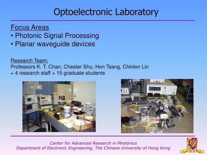
Optoelectronic Laboratory. Focus Areas Photonic Signal Processing Planar waveguide devices. Research Team: Professors K. T. Chan, Chester Shu, Hon Tsang, Chinlon Lin + 4 research staff + 15 graduate students. Examples of Research Output. All-optical signal processing Photonic ADC

E N D
Optoelectronic Laboratory • Focus Areas • Photonic Signal Processing • Planar waveguide devices Research Team: Professors K. T. Chan, Chester Shu, Hon Tsang, Chinlon Lin + 4 research staff + 15 graduate students
Examples of Research Output • All-optical signal processing • Photonic ADC • Polarization diversity loop for polarization insensitive operation • Wavelength conversion using • FWM in SOA • Birefringence Switching • Dual wavelength injection locking • Data Modulation Format Conversion (RZ to NRZ and NRZ to RZ) • OTDM demultiplexing • Waveguides • Polarization dependent frequency and polarization dependent loss compensation via • FIB trimming • Magnetostrictive layer deposited on waveguide • InGaAsP Waveguide Fabry-Perot filter (high speed tuneable via current injection) • Nonlinear Applications of SOI waveguides : Raman Amplification • Material properties (measure dispersion, Kerr effect & TPA in SOI waveguides) • Ultrafast optics and nonlinear optics • Spectral measurement in time domain using dispersion • Two photon autocorrelation using InGaAsP and Si waveguides • Terahertz pulse generation and detection using ion implanted GaAs T.K.Liang and H.K.Tsang, APPL PHYS LETT 81 (7): 1323 AUG 2002
Photonic ADC Lee KL, Shu C: “Switching-wavelength pulse source constructed from a dispersion-managed SOA fiber ring laser” IEEE PHOTONICS TECHNOLOGY LETTERS 15 (4): 513-515 APR 2003 / Fiber laser : electrical signal : optical signal • Sampling in optical domain and quantization in electronic domain Microwave signal quantization Optical Demux Digital signal processor Optical Source Sampling Transducer quantization Optical Source : Time and wavelength-interleaved pulses
10 Gigasample/s Photonic ADC using 10-wavelength sampling pulses • 10 channel output from • l1 = 1560.14 to • l10 = 1569.47 nm • Channel spacing: 1.03 nm • Suppression of non-lasing mode > 20 dB • Overall repetition rate: 10 GHz Individual loperated at 1 GHz • Pulse width: 21-26 ps • Timing jitter < 0.2 ps
PC4 SOA C1 PBS B PC1 PC5 OC 1 2 A C 3 D PC2 WDM PC3 Demultiplexer Isolator Pump 2 (P2) l l l Converted Pump 1 (P1) Signal (S) P1 C s Signal l P2 -5.0 -6.0 -7.0 -8.0 log(BER) -9.0 0.9 dB -10.0 Back-to-back -11.0 Converted -12.0 -36 -34 -32 -30 -28 -26 Received optical power (dBm) All-optical wavelength conversion 40 Gb/s wavelength conversion M.W.K. Mak, H.K. Tsang and K.Chan: “Widely tunable polarization-independent all-optical wavelength converter using a semiconductor optical amplifier,” IEEE Phot. Tech. Lett., vol.12, 525-527 (2000)
Pump 1 SOA Output Signal Pump 2 Wavelength conversion: BOPFWM without external optical pump K. K. Chow, C. Shu, M. W. K. Mak and H. K. Tsang, “Widely tunable wavelength converter using a double-ring fiber laser with a semiconductor optical amplifier,” IEEE Photonics Technology Letters, vol. 14, pp. 1445-1447, October 2002.
Tunable 40Gbit/s optical source C 3 1 2 Optical Coupler HDF PC1 OC Output FPLD SOA FFP PC2 Isolator RF Synthesizer Dispersive frequency Mode-locked SOA multiplication fiber-ring laser Mark W.K.Mak and H.K.Tsang: “Dispersive Frequency Multiplication for Wavelength-Tunable High Repetition Rate Pulse-Train Generation,”Optical Fiber Communications 2001 (Anaheim), 2001.
Optical CDMA Wang X, Lee KL, Shu C, Chan KT: “Multiwavelength self-seeded Fabry-Perot laser with subharmonic pulse-gating for two-dimensional fiber optic-CDMA,” IEEE PHOTONICS TECHNOLOGY LETTERS 13 (12): 1361-1363 DEC 2001
High speed tunable filter • Tunable waveguide filter H.K. Tsang et al. “ Etched Cavity InGaAsP/InP Waveguide Fabry-Perot Filter Tunable by Current Injection,” IEEE J. Lightwave Tech, vol.17, p.1890-1895 (1999)
y x Polarization compensation by magnetostriction Magnetostriction: anisotropic strain induced by magnetic field Saturation Magnetostriction constant (l) =fractional change in length External Magnetic field direction Ferromagnetic film Thermal oxide Thermal oxide Silicon Silicon Buried Oxide Buried Oxide Silicon Silicon P.S. Chan, H.K. Tsang, “Magnetostrictive Polarization Compensation on SOI Rib Waveguide”, 8th OptoElectronics and Communications Conference, Shanghai, China, Oct 2003.
Side view of trimmed portion of rib. Gallium Ion Focused Ion Beam Etching for mode conversion and PDF adjustment Top view of trimmed rib SOI waveguide by 45 degrees, 10mm Output TE power (dBm) TM -6 -8 WITHOUT compensation -10 -12 Compensated by 10um FIB -14 trimming -16 1550.02 1550.06 1550.10 1550.14 1550.18 Wavelength (nm) P.S. Chan, H.K. Tsang, C. Shu, “Mode Conversion and Birefringence Adjustment via Focused Ion Beam Etching for Slanted rib Waveguide walls”, to appear in Optics Lett. Nov. 2003.
Silicon oxynitride switch trench for liquid crystal material for switching A Zhang and KT Chan “Characterization of the optical loss of an integrated silicon oxynitride optical switch structure,” Appl. Phys. Lett., Vol. 83, No. 13, 29 September 2003
SiO2 Si p+ n+ Si (substrate) Stokes l (nm) DFB Laser waveguide Coupler Power Meter Monochrometer New topics of current interest • Raman gain in silicon waveguides (HK Tsang) • Quantum encryption using multiphoton entanglement generated from spontaneous parametric down conversion (KT Chan) • Photonic Crystal Fibers for signal processing and sensors (CT Shu)
Future Directions in planar waveguides & nanophotonics • Possible future directions: • Miniaturization of planar waveguide components using silicon wires • Requires considerable investment to improve dry etching capability (HKUST equipment is inadequate for etching submicron waveguides) • Work needed on improving coupling loss and polarization dependence • Periodic structures (thin film photonic crystal)? From Richard M. De La Rue “Photonic Crystal and Photonic Wire Devices and Technology” ECOC 2003 “The technological problems involved in fabrication with sufficient precision and acceptable propagation losses continue to present a major challenge for device engineers and physicists.” “… the likely impact of photonic crystal and photonic wire…is considerable. Within a small number of years, we are likely to witness moderately high volume production of devices which will incorporate the thinking that has been developed over a period of sixteen or more years”
Photonic Packaging Laboratory • A 3-year project with $12.334 million total funding from ITF and sponsors Project period: June 2001- May 2004 Funded by: • Major Equipment: • Optical Thin Film Coating System • Laser Welder • Automated Alignment System • Polishing System • Auto-Stepback Wedge Bonder • Precision Die Bonder • Wafer scriber
Photonic Packaging Laboratory • Mission: • To help build a photonic packaging infrastructure in Hong Kong by: • support R&D in industry and academia; • technical training; • facilitate technology transfer to industry. Technical Team: 13 engineering faculty staff from IE, EE, and ACAE departments, plus 3 full-time technical staff (Dr. Ming Li, April PS Chung, MT Yeung) PI : Hon Tsang, Chester Shu Coordinator: Frank Tong
Milestone 1 – Fiber attach and basic optical coatings Completed 31/7/2002 Packaged Components: Lasers, Photodetectors Butterfly FP/DFB laser module Pigtailed TO-Can photodetector • AR and HR coated FP Laser 1 Gb/s
Milestone 2: High Specification Coatings Completed 28/2/2003 • AR coatings (<0.05% reflectivity) on Si and III-V semiconductors • HR overlay coatings to enhance reflection and reduce PDL from gold mirrors
Collimating fiber Bonding pads Supporting Si Si U-grove / V-grove Input 1 Input 2 Si optical bench Glass MEMS Output 1 Output 2 Milestone 4: Fiber array attachment and MEMS packaging due 30/11/2003
Laser die Side alignment pedestal solder Plated Ni/Au Ti/Au/Ti/SiO2 Substrate waveguide Laser chip Side alignment pedestals Milestone 5: Multi-component packaging due 31/5/2004 • Development of novel self-aligned flip-chip technology for hybrid integration of laser arrays to planar waveguides • Collaboration with Institute of Semiconductors, Chinese Academy of Sciences in Beijing on fabrication of compatible FP laser array • Collaboration with Shipley on photoresist suitable for 3D topography (needed for patterning metal at bottom of trench