Download
1 / 55
580 likes | 654 Views
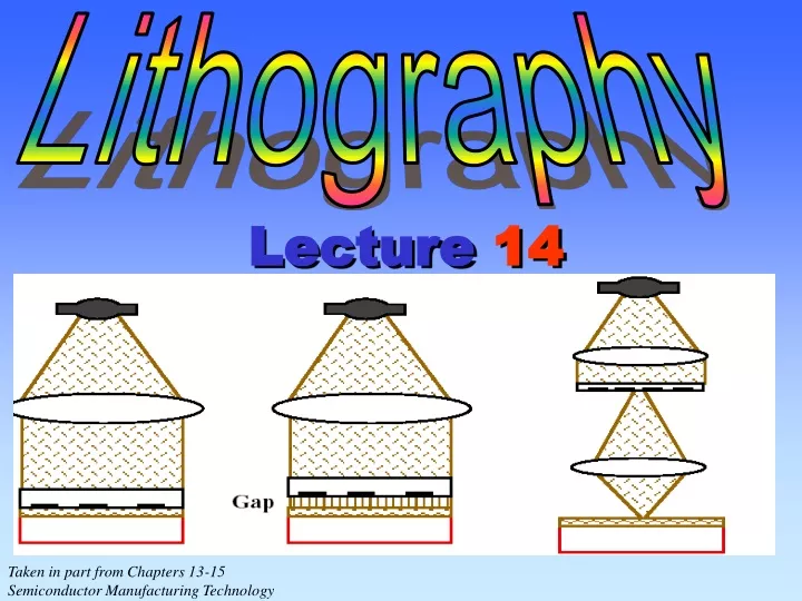
Lithography. Lecture 14. Taken in part from Chapters 13-15 Semiconductor Manufacturing Technology by Michael Quirk and Julian Serda. Basic concepts for photolithography, including process overview, critical dimension generations, light spectrum, resolution and process latitude.

E N D
Lithography Lecture 14 Taken in part from Chapters 13-15 Semiconductor Manufacturing Technology by Michael Quirk and Julian Serda
Basic concepts for photolithography, including process overview, critical dimension generations, light spectrum, resolution and process latitude. Difference between negative and positive lithography. Eight basic steps to photolithography. Wafer surface preparation for photolithography. Photoresist physical properties. Applications of conventional i-line photoresist. Deep UV resists Photoresist application techniques Soft bake processing Objectives
Wafer fabrication (front-end) Wafer start Thin Films Polish Unpatterned wafer Diffusion Photo Etch Completed wafer Test/Sort Implant Wafer Fabrication Process Flow
Patterning process Photomask Reticle Critical dimension generations Light spectrum and wavelengths Resolution Overlay accuracy Process latitude Photolithography Concepts
Three Basic Exposure Methods 1:1 Exposure 1:1 Exposure ~5:1 Exposure
Contact printing capable of high resolution but has unacceptable defect densities. May be used in Developmentbut not manufacturing. • Proximity printing cannot easily print features below a few mm in line width. Used in nano-technolgy. • Projection printing provides high resolution and low defect densities and dominates today. Typical projection systems use reduction optics (2X - 5X), step and repeat or step and scan. They print » 50 wafers/hour and cost $5 - 10M.
Steps in Lithography Process Lithography has three parts: (1) Light source, (2) Wafer exposure (3) Resist
1:1 Mask 4:1 Reticle Photomask and Reticle for Microlithography
Space Linewidth Photoresist Thickness Substrate Three Dimensional Pattern in Photoresist
Visible Micro- waves X-rays Gamma rays Infrared Radio waves UV 10 10 10 10 10 10 10 10 10 10 22 20 18 16 14 12 10 8 6 4 f (Hz) 10 10 10 10 10 10 10 10 10 10 (m) -14 -12 -10 -8 -6 -4 -2 0 2 4 193 365 436 157 248 405 l (nm) DUV DUV VUV h i g Common UV wavelengths used in optical lithography. Section of the Electromagnetic Spectrum
Decreasing feature sizes requires shorter λ. Hg vapor lamps: Hg plasma inside glass lamp Produces multiple wavelengths Limited in intensity “g” line: λ = 436 nm (used to mid 1980s) “I” line: λ = 365 nm (early 1990s, >0.3 μm) Deep UV by excimer lasers Kr + NF3 + (energy) → KrF + (photon emission) KrF: λ = 248 nm (used for 0.25 μm) ArF: λ= 193 nm (used for 0.12 μm) Light Sources
Important Wavelengths for Photolithography Exposure Table 13.1
Top view of CMOS inverter The masking layers determine the accuracy by which subsequent processes can be performed. The photoresist mask pattern prepares individual layers for proper placement, orientation, and size of structures to be etched or implanted. Small sizes and low tolerances do not provide much room for error. PMOSFET NMOSFET Cross section of CMOS inverter Importance of Mask Overlay Accuracy Figure 13.4
Negative Resist Wafer image is opposite of mask image Exposed resist hardens and is insoluble Developer removes unexposed resist Positive Resist Mask image is same as wafer image Exposed resist softens and is soluble Developer removes exposed resist Photolithography Processes
Ultraviolet light Areas exposed to light become crosslinked and resist the developer chemical. Chrome island on glass mask Island Exposed area of photoresist Window Photoresist Shadow on photoresist Photoresist Oxide Oxide Silicon substrate Silicon substrate Resulting pattern after the resist is developed. Negative Lithography
Ultraviolet light Areas exposed to light are dissolved. Chrome island on glass mask Shadow on photoresist Island Window photoresist Photoresist Exposed area of photoresist Photoresist photoresist Oxide Oxide oxide oxide silicon substrate Silicon substrate Silicon substrate silicon substrate Resulting pattern after the resist is developed. Positive Lithography
Island of photoresist Desired photoresist structure to be printed on wafer Substrate Chrome Quartz Window Island Mask pattern required when using positive photoresist (same as intended structure) Mask pattern required when using negative photoresist (opposite of intended structure) Relationship Between Mask and Resist
Clear Field Mask Dark Field Mask Simulation of metal interconnect lines (positive resist lithography) Simulation of contact holes (positive resist lithography) Clear Field and Dark Field Masks
UV Light HMDS Resist Mask 3) Soft bake 2) Spin coat 4) Alignment and Exposure 1) Vapor prime 6) Develop 5) Post-exposure bake 7) Hard bake 8) Develop inspect Eight Steps of Photolithography
The First Step of Photolithography: Promotes Good Photoresist-to-Wafer Adhesion Primes Wafer with Hexamethyldisilazane, HMDS Followed by Dehydration Bake Ensures Wafer Surface is Clean and Dry Vapor Prime
Process Summary: • Wafer is held onto vacuum chuck • Dispense ~5ml of photoresist • Slow spin ~ 500 rpm • Ramp up to ~ 3000 to 5000 rpm • Quality measures: • time • speed • thickness • uniformity • particles and defects Photoresist dispenser Vacuum chuck To vacuum pump Spindle connected to spin motor Spin Coat
Characteristics of Soft Bake: Improves Photoresist-to-Wafer Adhesion Promotes Resist Uniformity on Wafer Improves Linewidth Control During Etch Drives Off Most of Solvent in Photoresist Typical Bake Temperatures are 90 to 100°C For About 30 Seconds On a Hot Plate Followed by Cooling Step on Cold Plate Soft bake
Process Summary: • Transfers the mask image to the resist-coated wafer • Activates photo-sensitive components of photoresist • Quality measures: • linewidth resolution • overlay accuracy • particles and defects UV light source Mask Resist Alignment and Exposure
Required for Deep UV Resists Typical Temperatures 100 to 110°C on a hot plate Immediately after Exposure Has Become a Virtual Standard for DUV and Standard Resists Post-Exposure Bake
Process Summary: • Soluble areas of photoresist are dissolved by developer chemical • Visible patterns appear on wafer - windows - islands • Quality measures: - line resolution - uniformity - particles and defects Develop dispenser Vacuum chuck To vacuum pump Spindle connected to spin motor Photoresist Development
A Post-Development Thermal Bake Evaporate Remaining Solvent Improve Resist-to-Wafer Adhesion Higher Temperature (120 to 140°C) than Soft Bake Hard Bake
Inspect to Verify a Quality Pattern Identify Quality Problems (Defects) Characterize the Performance of the Photolithography Process Prevents Passing Defects to Other Areas Etch Implant Rework Mis-processed or Defective Resist-coated Wafers Typically an Automated Operation Develop / Inspect
Wafer Cleaning Dehydration Bake Wafer Priming Priming Techniques Puddle Dispense and Spin Spray Dispense and Spin Vapor Prime and Dehydration Bake Vapor Prime
Resist liftoff Effect of Poor Resist Adhesion Due to Surface Contamination
Spin wafer to remove excess liquid Puddle formation HMDS Puddle Dispense and Spin
Process Summary: • Dehydration bake in enclosed chamber with exhaust • Hexamethyldisilazane (HMDS) • Clean and dry wafer surface (hydrophobic) • Temp ~ 200 to 250C • Time ~ 60 sec. Chamber cover Wafer Hot plate Exhaust HMDS Hot Plate Dehydration Bake and Vapor Prime
To transfer the mask pattern to the photoresist on the top layer of the wafer surface To protect the underlying material during subsequent processing e.g. etch or ion implantation. Purpose of Photoresist in Wafer Fab
Better image definition (resolution). Better adhesion to semiconductor wafer surfaces. Better uniformity characteristics. Increased process latitude (less sensitivity to process variations). Progressive Improvements in Photoresist
Photoresist Types of Photoresist Negative Versus Positive Photoresists Photoresist Physical Properties Conventional I-Line Photoresists Negative I-Line Photoresists Positive I-Line Photoresists Deep UV (DUV) Photoresists Photoresist Dispensing Methods Spin Coat
Two Types of Photoresist Positive Resist Negative Resist CD Capability Conventional Resist Deep UV Resist Process Applications Non-critical Layers Critical Layers Types of Photoresists
Negative Resist Wafer image is opposite of mask image Exposed resist hardens and is insoluble Developer removes unexposed resist Positive Resist Mask image is same as wafer image Exposed resist softens and is soluble Developer removes exposed resist Resolution Issues Clear Field Versus Dark Field Masks Negative Versus Positive Resists
Resolution Contrast Sensitivity Viscosity Adhesion Etch resistance Surface tension Storage and handling Contaminants and particles Photoresist Physical Characteristics
Poor Resist Contrast • Sloped walls • Swelling • Poor contrast Good Resist Contrast • Sharp walls • No swelling • Good contrast Resist Resist Film Film Resist Contrast
Low surface tension High surface tension from low molecular from high molecular forces forces Surface Tension
Solvent: gives resist its flow characteristics Resin: mix of polymers used as binder; gives resist mechanical and chemical properties Sensitizers: photosensitive component of the resist material Additives: chemicals that control specific aspects of resist material Components of Conventional Photoresist Figure 13.18
Areas exposed to light become crosslinked and resist the developer chemical. Unexposed areas remain soluble to developer chemical. UV Photoresist Oxide Substrate Unexposed Exposed Soluble Crosslinks Pre-exposure - photoresist Post-exposure - photoresist Post-develop - photoresist Negative Resist Cross-Linking
Resist exposed to light dissolves in the developer chemical. Unexposed resist, containing PACs, remain crosslinked and insoluble to developer chemical. UV Photoresist Oxide Substrate Exposed Unexposed PAC Soluble resist Post-exposure + photoresist Post-develop + photoresist Pre-exposure + photoresist PAC as Dissolution Inhibitor in Positive I-Line Resist
Positive Photoresist: • Sharp walls • No swelling • Good contrast Resist Film Good Contrast Characteristics of Positive I-line Photoresist
KrF laser emission spectrum Emission spectrum of high-intensity mercury lamp 100 80 60 40 20 0 120 100 80 60 40 20 0 i-line 365 nm g-line 436 nm h-line 405 nm Relative Intensity (%) Relative Intensity (%) DUV* 248 nm 248 nm 200 300 400 500 600 Wavelength (nm) DUV Emission Spectrum * Intensity of mercury lamp is too low at 248 nm to be usable in DUV photolithography applications. Excimer lasers, such as shown on the left provide more energy for a given DUV wavelength.
Resist exposed to light dissolves in the developer chemical. Unexposed resist remains crosslinked and PAGs are inactive. UV Photoresist Oxide Substrate Exposed Unexposed PAG H+ PAG PAG PAG H+ PAG H+ PAG PAG PAG PAG Acid-catalyzed reaction (during PEB) Unchanged Pre-exposure + CA photoresist Post-exposure + CA photoresist Post-develop + CA photoresist Chemically Amplified (CA) DUV Resist
Exposure Steps for Chemically-Amplified DUV Resist Table 13.5
1) Resist dispense 2) Spin-up 3) Spin-off 4) Solvent evaporation Steps of Photoresist Spin Coating