Download
1 / 40
400 likes | 509 Views
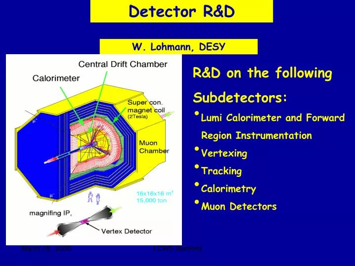
Detector R&D. W. Lohmann, DESY. R&D on the following Subdetectors: Lumi Calorimeter and Forward Region Instrumentation Vertexing Tracking Calorimetry Muon Detectors. A New Detector ‘ Scale ’. Impact Parameter: 1/3 х SLD (secondary vertices) 1/5-10 x LEP. Small beampipe

E N D
Detector R&D W. Lohmann, DESY R&D on the following Subdetectors: • Lumi Calorimeter and Forward • Region Instrumentation • Vertexing • Tracking • Calorimetry • Muon Detectors LCWS Stanford
A New Detector ‘Scale’ Impact Parameter: 1/3 х SLD (secondary vertices) 1/5-10 x LEP • Small beampipe • Low material budget • 4-5 layer structure Momentum resolution 1/10 x LEP • Single hit resolution • Number of hits • High B field Jet energy resolution 1/3 х LEP, HERA • Fine granularity compact calorimeters • single particle shower reconstruction • and particle flow approach Hermeticity > 5 mrad Dedicated Detector R&D needed
PhysicsRequirements for a Detector Major Goal: Explore Elektroweak Symmetry Breaking A light Higgs Boson: Identification of the Higgs (Mass, Spin, Parity), Couplings e+e- Z H l+ l- X (‘golden physics channel’), with d(ml+l-) << GZ Spin, Parity CP Mass accuracy ~40 MeV Higgs Field Potential, l b-tagging, t -tagging Jet energy resolution, b-tagging, vertex charge Momentum and jet energy resolution
Or, no Higgs Boson: Strong Interactions of Gauge Bosons sE/E = 0.6/sqrt(E) sE/E = 0.3/sqrt(e) -Reconstruction of the W’s from the measured Jet energies and directions Separation of WW and ZZ final states! and then search for technicolor
Detector Hermeticity SUSY: Detection of l , sleptons for small m ~ 10 fb ~ 106 fb • Detection of • high energy • electrons at • small angles • necessary
Very Forward Detectors Beamstrahlung Depositions: 20 MGy/year Rad. hard sensors e.g. Diamond/W BeamCal • Measurement of the Luminosity with precision (<10-3)using Bhabha scattering • Detection of Electrons and Photons at very low angle – extend hermeticity • Fast Beam Diagnostics 300 cm VTX FTD LumiCal IP Silicon/W sandwich LumiCal: 26 < q < 82 mrad BeamCal: 4 < q < 28 mrad PhotoCal: 100 < q < 400 mrad BeamCal L* = 4m
Simulation and sensor tests Beam test of diamond sensors Electron ID efficiency, BeamCal q resolution and bias in LumiCal 0.13e-3 rad 0.11e-3 rad Diamond response Bhabha scattering,full sower similation, weight cut intensity
Labs active in the three Regions Simulations General design Sensor Tests But, to be, frank, we are at the very beginning
Vertex Detector • Space Point Resolution < 4mm • Impact Parameter Resolution (d(IP) = 5 10/p sin3/2q) mm • Vertex Charge Measurement Transparent, < 0.1 % X0 per layer Small beam pipe Radius, < 15 mm thin walled beam pipe
Vertex Detectors Concepts under Development: • Charge Coupled Devices, CCD (demonstrated at SLD) • Fine Pixel CCD, FPCCD • DEpleted P-channel Field Effect Transistor (DEPFET) • Monolithic Active Pixel (CMOS), MAPS • Silicon on Insulator, SoI • Image Sensor with In-Situ Storage (ISIS) • Hybrid Pixel Sensors (HAPS) • ……. 11 technologies, 26 Groups around the world
DEPFET MIP source top gate drain clear bulk n+ p+ p+ n+ n+ p s n i x internal gate a + - - y - - - r t - - e + m m - y s + - n + - p+ rear contact Bonn, Mannheim,Munich 50 µm • Full Prototype System built, tested in the Lab and Testbeam Pixel size 20 x 30 mm2, 64 x 128 pixel • Thinning to 50 mm demonstrated • Rad. Hardness tested to 1 Mrad (60Co) • Readout with 100 MHz, Noise tolerable • Low Power Consumption (5W for a five Layer Detector)
Next Step: Design and produce a 512 x256 Pixel matrix
CCD The first Column parallel sensor and readout chip is operated (LCFI-CCD Collaboration) Clock Frequency ~ 25 MHz 750 x 400 pixels 20 m pitch CPR1 CPR1 20 mm pitch possible New Technologies: R&D issues: • Readout speed 50 MHz • Full size ladders (beam test 2010) • Fine Pixel CCD (Japan) • ISIS • (immune against EMI)
MAPS Mimosa-9 (Strasbourg) S/N ~ 24 Testbeam results • 20 mm sensitive layer • 20, 30, 40 mm pitch A 1 Mpixel sensor backthinned to 15 mm Prototype ladder in 2005 ?
Labs involved from the three Regions Exchange of informations between the groups (phone meetings)
Central Tracker Gaseous or Silicon s(1/p) = 6 x 10⁻⁵ GeV-1 • Design Studies (GossamerTracker) • (Resolution, Track Efficiency) • Long Silicon Strip sensors (Barrel) • Si Drift sensors (Forward) • Mechanical Support (<1% X0 per layer • FE Electronics (low noise, digitisation) • Field Cage- homogeneous E field • Mechanical Frame (< 3% X0) • Novel Gas Amplification System • Gas Mixture • Performance at High B –Field (100mm (Rf) Resolution)
Central Tracker- TPC Signal collection by pads or MediPix Gas amplification: Micromegas, GEMs
Examples of Prototype TPCs Carleton, Aachen, Desy(not shown) for B=0 studies Desy, Victoria, Saclay (fit in 2-5T magnets)
Point resolution, GEM • 2x6mm^2 pads. • In Desy chamber triple GEM • is used • In Victoria chamber a double GEM • In general (also for Micromegas) the resolution is not as good as expected from simulations • we are searching for why (electronics, noise, method). B=4T Gas:P5 30cm
π2beam line Beam Test@ KEK B = 0, 1 T 30cm
TPC, status and next steps: • A large international Community is engaged in TPC R&D • Both GEMs and MICROMEGAS seem to work • Construction of a ‘Large Prototype’ • Full System Test with the ‘Large Prototype’ in a beam A Collection of ongoing R&D topics: • Choice of gas mixture • (Diffusion, D-velocity) • Ion feedback • Readout electronics (pad density) • neutron background
SID/SiLC Simulations Mechanics Design FE and readout chip prototype (.18mm UMC) 16 channel pream, shaper. ADC) Lab. Tests are promising
SID/SiLC Ladder/Disk prototypes LPNHE test bench SiLC plans testbeam measurements with a prototype ladder in the fall of 2006 • Close contacts between N.A. and European groups • Exchange of designs for detector and electronics • Joint effort in simulations • Common testbeam measurement
Labs involved from the three Regions TPC SID/SiLC
FORWARD TRACKING +SIT :s(1/p) = 0.5 x 10⁻⁴ GeV-1 • SIT: Silicon strips • FTD: Silicon disks • FTC: Straw tubes, GEMs Design studies in DESY/JINR R&D in Louisiana Tech. Univ., 10 x 10 cm2 prototypes, Tests with Cosmics or: SiLC Components
Calorimetry ‘Particle’ flow concept requires to identify showers of individual particles in a jet Separation of ‘neutral’ and ‘charged’ depositions Charged particles in a jet are most precisely measured in the tracker Charged cluster Summing up the the energy measurement from tracking (charged), ECAL and HCAL(neutrals) : Neutral cluster D E /E = 30%/ sqrt(E) for jets! Neutral Kaon Granularity (longitudinal and transversal) (1x1 cm2) Compactness (small X0, RM) Mip detection (charged particle tracking) Photon direction measurement (‘imaging’) Charged Pion Showers of the neutral Pion →→+o
ECAL Si/W Technology Alveolus Tungsten Carbon fiber Detector slab Calice Si Sensors 1x1 cm2 5 inch waver manufactred in Korea 6 inch waver manufactred in US BNL/SLAC/Oregon • 5 mm pads (1/2 RM) • Each 6 inch waver is • readout by one chip • Electronics under way • Test beam in 2005
Univs. From Korea Testbeam measurements: DESY, CERN Calice Detector slab Top First Results will be soon available e- 3 GeV Front Side
ECAL Other Technologies 11.1%E e- LCcal: Scintillator/Si Hybrid EE Testbeam results: LCcal:First Cal in a testbeam! 45 layers Sci/Pb 3 planes Si pads Ebeam (GeV) Hi granularity Scintillator SiPM from Hammatsu, to be used eadout of Scintillator blocks Scintillator Strip/WLS Testbeam Prototype Cal end 2007
Sci/Pb Technology KEK beam: 1 – 4 GeV e, m, p shower profile, data-MC comparison calorimetric angular measurement
HCAL – Analog or Digital Steel-Scintillator Sandwich HCAL with SiPM readout Large area layers equipped with SiPMs ’MiniCal Prototype
1 m3 Tile HCAL prototype Readout Elecronics First Tests with hadron test beam in 2005/6
HCAL – Analog or Digital 3mm side walls and spacers installed GEM Digital Cal Embeded onboard readout Development of large area GEM foils (Arlington) 50GeV Analog 50GeV Digital Promising results from Simulations
Pad array 1.1mm Glass sheet 1.1mm Glass sheet -HV Aluminum foil RPC Digital Cal Example: ANL Size: 30x100 cm2 • About 10 RPC prototypes of • different design built • Multichannel digital readout system • Large Size RPC with exellent • performane • Ready to built RPCs for a 1 m3 • prototype cal
Labs involved from the three Regions • CALICE includes institutes from all regions • N.A. groups and CALICE plan a joint testbeam program at FNAL
Muon Detection Instrumentation of the Iron of the Magnet – Large area detectors Technologies: • RPCs • Scintillation counter strips Improves The resolution of the HCAL
Status in R&D The nice things: • Lots of activities in all subdetectors • Simulations to optimise the design of • all components are ongoing • Mechanics design studies under way • Readout concepts are designed and under test • Testbeam studies are done for many sensors, but • not yet all • A few prototype detectors started studies • with testbeams
Status in R&D The challenges left: • There are essential parameters to be better understood • Testbeam studies must be extended to all sensor • types • Testbeam studies for prototypes of all subdetectors are • the Major Topic for the next years- • the only way to proove of performance goals • Testbeam results are input for refined simulations- • improved designs or redesigns • ‘Full system’ tests must be done • Prototypes and testbeams need a new level • of funding • I am sure I forgot something
Time Schedule 2004 2005 2006 2007 2008 2009 2010 (Construction) GDI (Design) Technology Choice Acc. CDR TDR Start Global Lab. Detector Outline Documents CDRs LOIs Det. Done! WWS Detector R&D Panel Collaboration Forming R&D Phase Construction Tevatron SLAC B HERA LHC T2K Taken from Y. Sugimoto
Conclusion Its timely to organise our community world wide to strengthen and structure the efforts in ILC Detector R&D Charge of the LC Detector R&D Panel: • creation of a register of ongoing R&D programs • Survey the R&D relevant for LC experiments • Critically review the status of R&D • Facilitate the review of R&D proposals The following people supported the preparation of this talk and I would like to thank them: P. Checcia, Ch. Damerell, R. Fray, HongJoo, D. Peterson, A. Savoy-Navarro, R. Settles, Y. Sugimoto, M. Trimpl, H. Weerts, N. Wermes, …..