Download
1 / 66
690 likes | 950 Views
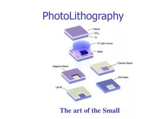
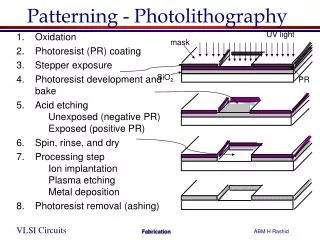
Small Feature Reproducibility A Focus on Photolithography. UC-SMART Major Program Award Spanos, Bokor, Neureuther Second Annual Workshop 11/8/99. Agenda. 8:30 – 9:00 Introductions, Overview / Spanos 9:00 – 10:15 Lithography / Spanos, Neureuther, Bokor 10:15 – 10:45 Break

E N D
Small Feature ReproducibilityA Focus on Photolithography UC-SMART Major Program Award Spanos, Bokor, Neureuther Second Annual Workshop 11/8/99 SFR Workshop - Lithography
Agenda 8:30 – 9:00 Introductions, Overview / Spanos 9:00 – 10:15 Lithography / Spanos, Neureuther, Bokor 10:15 – 10:45 Break 10:45 – 12:00 Sensor Integration / Poolla, Smith, Solgaard, Dunn 12:00 – 1:00 lunch, poster session begins 1:00 – 2:15 Plasma, TED / Graves, Lieberman, Cheung, Aydil, Haller 2:15 – 2:45 CMP / Dornfeld 2:45 – 3:30 Education / Graves, King, Spanos 3:30 – 3:45 Break 3:45 – 5:30 Steering Committee Meeting in room 775A / Lozes 5:30 – 7:30 Reception, Dinner / Heynes rm, Men’s Faculty Club SFR Workshop - Lithography
Litho Milestones, Year 1 • Demonstrate AFM aerial image inspection on 180nm features. • Demonstrate Specular Spectroscopic Scatterometry CD metrology for 180nm features. • Demonstrate focus classification scheme for 180nm features. • Complete 3D device simulations of mask errors and LER effects in gate-level. Threshold voltage shifts, turn-off characteristics, and saturated drain current will be evaluated. • Complete a simulation feasibility study and verification experiment on novel in-lens filtering for resolution enhancement. • Evaluate the physical basis for novel effects in interaction of light with materials and low voltage electrons with resists. • Establish web based simulation capabilities for DUV resists, mask topography effects and electron-beam lithography. SFR Workshop - Lithography
Litho Milestones, Year 2 • Demonstrate AFM aerial image inspection on 50nm features. • Demonstrate 150nm Specular Spectroscopic Scatterometry CD metrology. • Demonstrate focus classification scheme for 150nm features. • Test NMOS devices with programmed mask errors and LER, compare measured characteristics to simulation. • Integrate scattering, imaging, resist modeling for analyzing inspection and printabilty of mask non-idealities in the context of use with OPC. • Establish a prototype system for process integration including the automatic generation of simulation-designed multi-step, short loop test structures. • Establish web based simulation capabilities for optical alignmentand advanced electron-beam lithography. SFR Workshop - Lithography
Outline • Simulation and Metrology • Lithography Simulator Calibration • Scatterometry • Plans for Statistical Process Optimization • Line Edge Roughness • Lithography Simulation SFR Workshop - Lithography
Thickness Thickness Thickness CD, profile and n and k n and k n and k Thickness Exposure Spin Coat Thin film Develop & & PEB Soft Bak e In-situ / On-wafer thin film Metrology • Reflectometry / Ellipsometry / Scatterometry • Thickness, n & k, chemical composition • Run-to-run and real-time monitoring • Resist surface analysis for aerial image evaluation SFR Workshop - Lithography
Motivation for Parameter Extraction • Current lithography simulators are parameter limited as opposed to model limited. • Traditional optimization techniques are unsuitable in complex, non-linear, high dimensional problems. • Importance of predictive capabilities is increasing with increasing development costs and time-to-market pressures. SFR Workshop - Lithography
Some Critical Parameters in DUV Lithography Simulation Amplification Rate (Pre-exp) Amplification Rate (Activation) Acid Loss Rate (Pre-exp) Acid Loss Rate (Activation) Dill’s A Parameter Dill’s B Parameter Dill’s C Parameter Relative Quencher Conc. PEB Diffusivity (Pre-exp) PEB Diffusivity (Activation) Maximum Develop Rate Minimum Develop Rate Developer Selectivity Developer Threshold PAC Resist Refractive Index (Real) Resist Refractive Index (Imag.) ARC Refractive Index (Real) ARC Refractive Index (Imag.) Relative Focus Amplification Reaction Order • Exact values obtained from experiments or resist vendor • Narrow range of values available from unpatterned experiments • Wide parameter range SFR Workshop - Lithography
Proposed DUV-SCAPE Framework 3: user specified parameter ranges 2: global optimization engine (SAC) 1: unpatterned resist experiments 5: commercial simulation program 6: simulated profile 4: parameter interface front end 7: global optimization engine (SAC) 2: image processing front end 3: experimental profile 1: patterned resist experiments SFR Workshop - Lithography
Salient Features • Unpatterned Resist Models • BCAM exposure and bake models • Mack develop model • Optimization Technique • Global optimization theory (Adaptive Simulated Annealing) • Patterned Resist Model • Existing lithography simulators (e.g. SAMPLE, Prolith, Solid-C, etc.) SFR Workshop - Lithography
Experiments - Commercial DUV Resist • Unpatterned Resist Characterization Experiments • Process 4 wafers with flood exposed sites • Measure ARC and Resist optical constants - Ellipsometry • Measure exposure and PEB parameters - FTIR/DITL • Measure develop parameters - DRM • Patterned Resist Characterization Experiments • Process 1 wafer with a focus-exposure matrix • Measure profiles for sub-quarter micron lines using AFM/cross-section CD-SEM/Specular Spectroscopic Scatterometry SFR Workshop - Lithography
Unpatterned Experiments 1 .5 0 135C 140C Exposure + PEB Parameters Deprotection 120C 110C 0 1 2 3 4 5 6 7 Exposure Dose (mJ/cm2) 3000 Develop Parameters 2000 Develop Rate in A/sec 1000 0 0 0.5 1 Normalized concentration of unreacted sites SFR Workshop - Lithography
Patterned Experiments: AFM vs Simulation mask 1 mask 2 mask 3 mask 4 mask 5 mask 6 mask 7 mask 8 mask 9 mask 10 Masks 1-10 differ in the line-space ratios 0.25 micron process technology OPC assisted masks -1 Focus +1 -1 Focus +1 SFR Workshop - Lithography
What is Scatterometry? • Concept: Scattering (Diffraction) of light from features produces strong structure in reflected optical field. • Analyze structure to obtain topography information. • Periodic structures (gratings) can be numerically modeled “exactly”. Incident Laser Beam Incident Polarized White Light 0th order 0th order Specular Spectroscopic Scatterometry 2-q Scatterometry SFR Workshop - Lithography
0 +1 -1 i D Specular Spectroscopic Scatterometry 0th order, broadband detection 1D gratings and 2D symmetric gratings Use spectroscopic ellipsometers sinqm = sinqi+ml/D |sinqm|<1 l Cut-Off Pitch 600 300 400 200 250 125 (in nm) SFR Workshop - Lithography
Timbre ProfilerTM Flow Timbre ProfilerTM Timbre ProfilerTM Library Generation Electromagnetic Simulation Software Generate Profile Library Generate Signal Library Typical turnaround time = 6-12 hours Compiled Profiler Library Compiled Profiler Library Collect Reflected Signal Timbre ProfilerTM Measurement Reconstructed Profile Ellipsometer / Reflectometer Test Grating (Scribe Lane) Total Measurement + Analysis = 5 seconds/site Load Library on Ellipsometer Ellipsometry Measurement Analysis SFR Workshop - Lithography
ProfilerTM Setup • Periodic grating on mask (~ 50 mm * 50 mmarea - typical spot size of production spectroscopic ellipsometers) • line/space specified • Provide optical constants for each film in the stack • Broadband (240-800 nm) • Specify variability expected in process (in CD & thickness) • range around nominal in nm • Specify spectroscopic ellipsometer / reflectometer angle of incidence • Save broadband tan y and cos D values • Specify accuracy requirements • down to sub-nm (this automatically decides library size) SFR Workshop - Lithography
GTK Interface at http://sfr.berkeley.edu SFR Workshop - Lithography
Matching on tan(Y) and cos(D) Tan(Y) Cos(D) Simulated by GTK SFR Workshop - Lithography
Example of 0.25mm Profile Extraction Blue is actual (by Veeco AFM). Red is extracted from GTK Library. SFR Workshop - Lithography
Case I: Resist on ARC on Si (0.18 mm technology) Resist ARC Si Focus-Exposure Matrix SFR Workshop - Lithography
Profile Extraction over the entire FEM RED is AFM. BLUE is extracted. SFR Workshop - Lithography
Offset between CD-SEM and ProfilerTM as a function of Sidewall Angle D bottom CD (CDSEM - PXM) in nm Sidewall angle in degrees SFR Workshop - Lithography
Case II: Resist on ARC on Metal (0.25 mm technology) Focus-Exposure Matrix Resist ARC TiN Al TiN Ti TEOS Si SFR Workshop - Lithography
Profile Extraction: Resist on ARC on Metal CD-SEM (Bottom CD) Profiler Extraction PXM (Bottom CD) CD (in nm) Correlation* = 0.93 Site Number SFR Workshop - Lithography
Case III: Etched Metal TiN Al TiN Ti TEOS Si Focus-Exposure Matrix SFR Workshop - Lithography
Profile Extraction : Etched Metal CD-SEM (Top CD) Correlation = 0.92 CD (in nm) Profiler Extraction PXM (Top CD) Site Number SFR Workshop - Lithography
But What Is Our Real Goal? -- a good profile ? -- or high yield ? • We cannot avoid process variations • Recipe setting drift: focus ( ~0.2 m), dose, PEB temperature • Model and material parameter variation: resist n & k, developer Rmax and Rmin, acid diffusivity • System inherent variation: mask OPC feature variation • Our goal is to maximize yield for the statistical distribution of parameters and operating points. SFR Workshop - Lithography
Parameter Variation Effect Profile deviation from best setting Operating Point Settings SFR Workshop - Lithography
Parameter and Operating Point Variances Extraction Parameter mean + variation Recipe setting + drift Lithography process Experiment data In-die spatial variation Hierarchical process disturbance extraction SFR Workshop - Lithography
Recipe Optimization with Variations Parameter distributions Spatial variation Simulated Output distributions Profiles within spec. Calibrated Lithography Simulator + - Operating Point distributions Overlapping to get yield RECIPE OPTIMIZER SFR Workshop - Lithography
Recipe Optimization with Multiple Feature Types • Poly layer • isolated line • periodic lines with OPC • metal layer • isolated line • periodic lines with OPC • elbows • combination of above • Need to link recipe optimization to circuit performance! SFR Workshop - Lithography
Parameter relationship analysis • In reality, all parameters have variations • too many dimensions for output distribution calculation • Parameter relations can be analyzed to attribute the variation of some parameters to other parameters • diffusivity PEB temperature • developer temperature Rmin and Rmax • What are the fundamental reasons behind the variation? • Need a comprehensive list of disturbances, linked to physical models, circuit performance. SFR Workshop - Lithography
Summary Experiment Data Spatial variation filter Param. & op. point variance Param. mean values Calibrated Sim. Eng. Target Specs. of features Recipe of max. yield In-line sensor measurement Maximization of overlapping area SFR Workshop - Lithography
What is Next? • Extend statistical optimization to other process steps • Plasma etching • Metallization • Device level • Circuit level • Process simulator for other steps needed • Simulator for full process procedure: Avant!, Solid C • device model: BSIM3 • Circuit simulator: SPICE • Study error budgets, linked to circuit performance. SFR Workshop - Lithography
Outline • Simulation and Metrology • Line Edge Roughness • Lithography Simulation SFR Workshop - Lithography
Defining LER and Defect Specifications SFR Workshop November 08, 1999 Tho Nguyen, Shiying Xiong and J. Bokor Berkeley, CA The objective of this work is to understand and model the impact of lithography/etch line-edge roughness in the gate definition layer, on the electrical behavior of short channel transistors SFR Workshop - Lithography
Progress Since May • Hydrodynamic Model working • 3D interaction of Defects • Real LER Simulation SFR Workshop - Lithography
Effect of Gate “Errors” on Device Characteristics gate • Threshold voltage • Turn-off slope • Drive current • Device reliability Cross-section n+ n+ Edge roughness Layout views DL Single defects DW SFR Workshop - Lithography
Base Design Channel Doping Selected at 0.4 Volt Halo Implant Incorporated to Offset Vt rolloff Threshold Swing 70-80 mV/decade @ Vds = 2V and L = 100nm DIBL = 70 mV/V for Vds = 0.05-2V Vt RollOff Characteristics 500 450 Device Length = 200 nm Channel Length = 100 nm Channel Width = 50-200 nm Buried Oxide = 100 nm Si Film Thickness = 250Å Gate Oxide = 30 Å 400 Without Halo Implant 350 With Halo Implant 300 250 0 0.2 0.4 0.6 0.8 1 1.2 Channel Length (Microns) SFR Workshop - Lithography
Real 3D LER Construction and Simulation • Real 3D LER Created by Matlab and incorporated into simulator language • LER defined by band-limited white spectrum. 2 parameters: RMS roughness, correlation length • Process simulation used for self-aligned S/D doping • Current digitized LER resolution is 0.5-1nm due to limited memory 160 SFR Workshop - Lithography
Simulation Results • Hydrodynamic model has been successfully turned on in ISE simulator • With hydro on, Ion is ~ 30% higher • Simulations of “real” 3D LER has been successful ( @ W = 50nm) I_V Curves for Different Real 3D LER Zoom View of Leakage Current • 25 % increase in Ioff for 5nm rms roughness • 140% increase in Ioff for 9nm rms roughness SFR Workshop - Lithography
Simulation Results • Defect shows 3D interaction for channel width less than 100nm • To study LER, we have to use 3D models • Intel Work (T. Linton, et al. 1999): • Simulation of square-wave modulation of LER with Neuman boundary conditions • Shows similar 3D interaction • Leakage control by length adjustment with reasonable Ion reduction SFR Workshop - Lithography
Milestone Status • June 1999 • Complete 3D device simulations of mask errors and LER effects in gate-level. Threshold voltage shifts, turn-off characteristics, and saturated drain current will be evaluated. • Status: Late. Student (Tho Nguyen) started Jan. 1999. Second student (Shiying Xiong) started Sept. 1999. Expect completion March 2000. • June 2000 • Test NMOS devices with programmed mask errors as well as varied LER and compare measured characteristics with simulation results. • Status: Delayed. No company fab support. Will start Microlab run Jan. 2000 if unable to arrange support from company fab. SFR Workshop - Lithography
Proposal for 2000-2002 • Simulation • Effect of LER on GIDL • Effect of LER in isolation edge • Device reliability • Extend to 50 nm CD • Experiments • Complete gate roughness experiment for 100 nm CD • Isolation roughness experiment • Extend to 50 nm CD?? SFR Workshop - Lithography
Outline • Simulation and Metrology • Line Edge Roughness • Lithography Simulation SFR Workshop - Lithography
Implications of Polarization, Corner Rounding, OPC Design and OPC Fidelity on Aerial Images Konstantinos Adam Prof. Andrew Neureuther UC Berkeley • Use EM theory and rigorous TEMPEST simulations to investigate photomask technology issues • Current Investigations • scattering bars - polarization effects • corners - interior versus exterior • OPC features - placement and corner rounding SFR Workshop - Lithography
Incident radiation CD SB y-axis mm mm z-axis x-axis Scattering Bar Simulation with TEMPEST l=193nm Mag=4X CDtarget=130nm |Ey| TE : Ey polarization |Ex| TM : Ex polarization mm mm SFR Workshop - Lithography
1.4 No SB 1.2 SPLAT TE 1 TM 0.8 0.6 0.4 SB size = 0.18l/NA 0.2 0 0 0.1 0.2 0.3 0.4 0.5 SB Aerial Images l=193nm, NA=0.7, s=0.6, Mag=4X, CDtarget=130nm Aerial Image (Best focus) Normalized Intensity (mm) - Observe that the scatter bars (also the main feature) appear wider in TM excitation than in TE and narrower with SPLAT simulation (scalar theory) SFR Workshop - Lithography
160 1 150 SPLAT SPLAT TE TE .8 TM TM 140 Perturbation model .6 130 .4 120 .2 110 0 0 0.1 0.2 0.3 0 0.05 0.1 0.15 0.2 0.25 0.3 0.35 SB Design Graphs Intensity dip of SB CD Control with SB Size Control Intensity CD (nm) Size of SB (l/NA) Size of SB (l/NA) SFR Workshop - Lithography