Download
1 / 1
10 likes | 111 Views
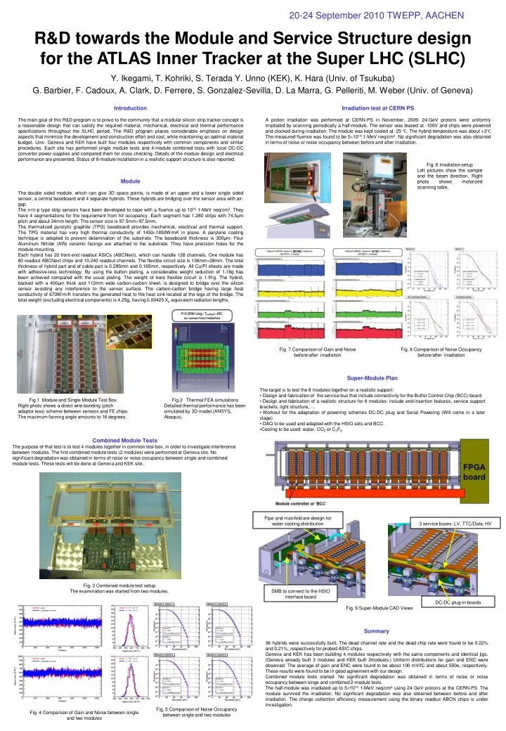
20-24 September 2010 TWEPP, AACHEN. R&D towards the Module and Service Structure design for the ATLAS Inner Tracker at the Super LHC (SLHC). Y. Ikegami, T. Kohriki, S. Terada Y. Unno (KEK), K. Hara (Univ. of Tsukuba)

E N D
20-24 September 2010 TWEPP, AACHEN R&D towards the Module and Service Structure designfor the ATLAS Inner Tracker at the Super LHC (SLHC) Y. Ikegami, T. Kohriki, S. Terada Y. Unno (KEK), K. Hara (Univ. of Tsukuba) G. Barbier, F. Cadoux, A. Clark, D. Ferrere, S. Gonzalez-Sevilla, D. La Marra, G. Pelleriti, M. Weber (Univ. of Geneva) Introduction The main goal of this R&D program is to prove to the community that a modular silicon strip tracker concept is a reasonable design that can satisfy the required material, mechanical, electrical and thermal performance specifications throughout the SLHC period. The R&D program places considerable emphasis on design aspects that minimize the development and construction effort and cost, while maintaining an optimal material budget. Univ. Geneva and KEK have built four modules respectively with common components and similar procedures. Each site has performed single module tests and 4-module combined tests with local DC-DC converter power-supplies and compared them for cross checking. Details of the module design and electrical performance are presented. Status of 8-module installation in a realistic support structure is also reported. Irradiation test at CERN PS A proton irradiation was performed at CERN-PS in November, 2009. 24-GeV protons were uniformly irradiated by scanning periodically a half-module. The sensor was biased at -100V and chips were powered and clocked during irradiation. The module was kept cooled at -25 ℃. The hybrid temperature was about +3℃. The measured fluence was found to be 51014 1-MeV neq/cm2. No significant degradation was also obtained in terms of noise or noise occupancy between before and after irradiation. Fig. 6 Irradiation setup Left picturesshow the sample and the beam direction. Right photo shows motorized scanning table. Module The double sided module, which can give 3D space points, is made of an upper and a lower single sided sensor, a central baseboard and 4 separate hybrids. These hybrids are bridging over the sensor area with air-gap. The n-in-p type strip sensors have been developed to cope with a fluence up to 1016 1-MeV neq/cm2. They have 4 segmentations for the requirement from hit occupancy. Each segment has 1,280 strips with 74.5μm pitch and about 24mm length. The sensor size is 97.5mm97.5mm. The thermalized pyrolytic graphite (TPG) baseboard provides mechanical, electrical and thermal support. The TPG material has very high thermal conductivity of 1450–1850W/mK in plane. A parylene coating technique is adopted to prevent delamination of the substrate. The baseboard thickness is 300μm. Four Aluminum Nitride (AlN) ceramic facings are attached to the substrate. They have precision holes for the module mounting. Each hybrid has 20 front-end readout ASICs (ABCNext), which can handle 128 channels. One module has 80 readout ABCNext chips and 10,240 readout channels. The flexible circuit size is 136mm28mm. The total thickness of hybrid part and of cable part is 0.295mm and 0.165mm, respectively. All Cu/PI sheets are made with adhesive-less technology. By using the button plating, a considerable weight reduction of 1.18g has been achieved compared with the usual plating. The weight of bare flexible circuit is 1.91g. The hybrid, backed with a 400μm thick and 112mm wide carbon-carbon sheet, is designed to bridge over the silicon sensor avoiding any interference to the sensor surface. The carbon-carbon bridge having large heat conductivity of 670W/m/K transfers the generated heat to the heat sink located at the legs of the bridge. The total weight (excluding electrical components) is 4.25g, having 0.00425 X0 equivalent radiation lengths. Fig. 7 Comparison of Gain and Noise before/after irradiation Fig. 8 Comparison of Noise Occupancy before/after irradiation • Super-Module Plan • The target is to test the 8 modules together on a realistic support: • Design and fabrication of the service bus that include connectivity for the Buffer Control Chip (BCC) board • Design and fabrication of a realistic structure for 8 modules: include end-insertion features, service support brackets, light structure, … • Workout for the adaptation of powering schemes DC-DC plug and Serial Powering (Will come in a later stage) • DAQ to be used and adapted with the HSIO sets and BCC • Cooling to be used: water, CO2 or C3F8 Fig.1 Module and Single Module Test Box Right photo shows a direct wire bonding (pitch adaptor less) scheme between sensors and FE chips. The maximum fanning angle amounts to 16 degrees. Fig.2 Thermal FEA simulations Detailed thermal performance has been simulated by 3D model (ANSYS, Abaqus). Combined Module Tests The purpose of that test is to test 4 modules together in common test-box, in order to investigate interference between modules. The first combined module tests (2 modules) were performed at Geneva site. No significant degradation was obtained in terms of noise or noise occupancy between single and combined module tests. These tests will be done at Geneva and KEK site. Pipe and manifold are design for water cooling distribution 3 service buses: LV, TTC/Data, HV Fig. 3 Combined module test setup The examination was started from two modules. SMB to connect to the HSIO interface board DC-DC plug-in boards Fig. 9 Super-Module CAD Views Summary 36 hybrids were successfully built. The dead channel rate and the dead chip rate were found to be 0.22% and 0.21%, respectively for probed ASIC chips. Geneva and KEK has been building 4 modules respectively with the same components and identical jigs. (Geneva already built 3 modules and KEK built 2moduels.) Uniform distributions for gain and ENC were observed. The average of gain and ENC were found to be about 100 mV/fC and about 550e, respectively. These results were found to be in good agreement with our design. Combined module tests started. No significant degradation was obtained in terms of noise or noise occupancy between singe and combined 2-module tests. The half-module was irradiated up to 51014 1-MeV neq/cm2 using 24 GeV protons at the CERN-PS. The module survived the irradiation. No significant degradation was also obtained between before and after irradiation. The charge collection efficiency measurement using the binary readout ABCN chips is under investigation. Fig. 5 Comparison of Noise Occupancy between single and two modules Fig. 4 Comparison of Gain and Noise between single and two modules