Download
1 / 34
350 likes | 475 Views
Optical AO WFS Detector Developments at ESO.

E N D
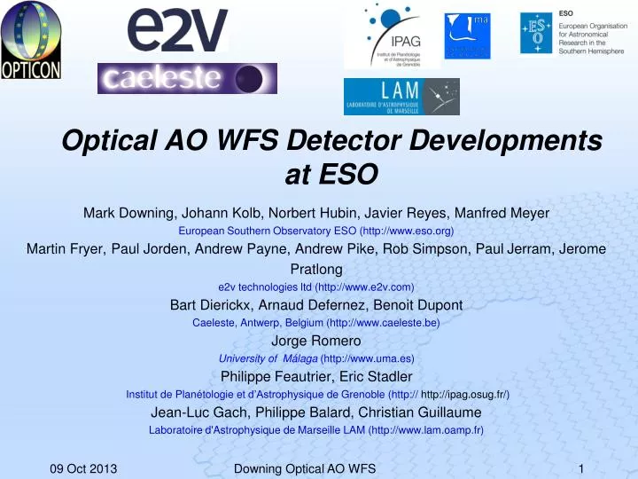
Optical AO WFS Detector Developmentsat ESO Mark Downing, Johann Kolb, Norbert Hubin, Javier Reyes, Manfred MeyerEuropean Southern Observatory ESO (http://www.eso.org)Martin Fryer, Paul Jorden, Andrew Payne, Andrew Pike, Rob Simpson, Paul Jerram, Jerome Pratlonge2v technologies ltd (http://www.e2v.com) Bart Dierickx, Arnaud Defernez, Benoit Dupont Caeleste, Antwerp, Belgium (http://www.caeleste.be) Jorge Romero University of Málaga (http://www.uma.es)Philippe Feautrier, Eric StadlerInstitut de Planétologie et d’Astrophysique de Grenoble (http:// http://ipag.osug.fr/) Jean-Luc Gach, Philippe Balard, Christian Guillaume Laboratoire d'Astrophysique de Marseille LAM (http://www.lam.oamp.fr) Downing Optical AO WFS
Outline • L3Vision CCD220 – developed by e2v on behalf of ESO/OPTICON • Deployment of AONGC Cameras on VLT AO instruments • Test Result Summary • Trades made with Deep Depletion CCD220 • Improvements of the HV Clock Design • SCTE • Next challenge → LGSD/NGSD • Large CMOS Visible AO WFS Imager for the ELT to sample the spot elongation of Laser Guide Stars • Specifications • Wavefront Sensor Architecture and Design • First results Downing Optical AO WFS
OP 4 Gain Registers 8 L3Vision Gain Registers/Outputs Each 15Mpix./s. Metal Buttressed 2Φ 10 Mhz Clocks for fast image to store transfer rates. Store slanted to allow room for multiple outputs. Store Area e2v L3Vision CCD220 OP 8 Gain Registers Image Area 240x120 24□µm Image Area 240x120 24□µm OP 3 OP 7 Store Area OP 6 OP 2 Gain Registers Gain Registers OP 1 OP 5 • e2v CCD220: • 240x240 24 µm pixels • Split frame transfer CCD • 8 L3Vision EMCCD outputs • < 0.1 e- RoNat1,500 fps • Integral Peltier for cooling to -50ºC Downing Optical AO WFS
Deployment of AONGC WFS Cameras MUSE HAWKI ERIS SPHERE Downing Optical AO WFS
CCD220 Impressive (Measured) Test Results • Key goal specs are met • Deep Depletion (highly sought after for better red response) is working as good as the standard silicon devices. • Next Steps: • Increase frame rate to 2,500 fps to extend use to E-ELT XAO (Extreme AO). • Test shuttered device CCD219 for pulsed laser guide star applications. Downing Optical AO WFS
Trades made with Deep Depletion Device • Deep Depletion enabled devices to be built out of thicker silicon (40µm) for better red response; • Highly sought after for applications using Natural Guide Stars. • 75% improvement Downing Optical AO WFS
Trades made with Deep Depletion Device • Deep Depletion enabled devices to be built out of thicker silicon (40µm) for better red response; • Highly sought after for applications using Natural Guide Stars. • During charge integration if the image area is simply run into inversion for lowest dark current like the Std Si device then obtain very poor PSF. • Has an additional “p” well implant for EMCCD to work. • A minimum bias is required to “punch-through” (depletion to extend beyond) this “p” well. Deep Depletion Std Si Downing Optical AO WFS
Trades made with Deep Depletion Device • Deep Depletion enabled devices to be built out of thicker silicon (40µm) for better red response; • Highly sought after for applications using Natural Guide Stars. • During charge integration if the image area is simply run into inversion for lowest dark current like the Std Si device then obtain very poor PSF. • Solution is to use Tri-Level clocking to obtain the best trade between PSF and Dark Current. • Low Level that takes the device into inversion for low dark current. • High Level just right for good frame transfer and low Clock Induced Charge. • Very High Level for integrating charge to tune the PSF. Integration Frame Transfer Very High Level Image Area Clock -0.5V High Level -8V Low Level Downing Optical AO WFS
Adjust Very High Level to Tune PSF VInteg=-8V VInteg=-4V VInteg=0V VInteg=4V VInteg=8V VInteg=12V Min met at > 2V. Goal met at > 8V. Min. Goal Min. Goal Downing Optical AO WFS
and trade with CIC and Dark Current • As expected CIC does not increase with integration voltage. • Once out of inversion, dark current does not increase further with integration voltage. • thanks to “Intrinsic dithering” – uses the fact that after inversion holes that have migrated into Si/SiO2 I/F have long release time constant. • Goal Dark Current and PSF specs are met at 8V. 1200fps 100fps Downing Optical AO WFS
Improvement to Design of HV Clock Peak Detector • Design → LC resonant circuit • switch, transformer, and capacitor (includes that of the CCD phases); • tune to resonate at pixel (switch) frequency; • simple, low power dissipation. • First implementation: • levels stabilized by simply correction for the integrated difference between peak and reference level. • Problem is that it does not respond quickly to transients/disturbances. • Both measurements and simulations prove that the resonance circuit is very sensitive to any changes in the load. The load (the CCD) changes during read out due to changes in clock (inter) capacitances. 20-50V Peak Detector ~ 0V ON OFF Tpixel Downing Optical AO WFS
At Unity Gain: Flat field is very flat Downing Optical AO WFS
However at gain, flat field varies with readout • Oscilloscope shows the amplitude of the HV Clock varies during a frame read out and variation is proportional to illumination level. Downing Optical AO WFS
Solution is to use full PID controller in the feedback loop • A properly designed PID controller should respond quickest to disturbances. Peak Detector PID Peak Detector PID Downing Optical AO WFS
Original design with step input Downing Optical AO WFS
Optimised design with step input Downing Optical AO WFS
“Proof of the Pudding” Afterwards Before Downing Optical AO WFS
SCTE - Long Tail of Residual Charge Store section 60 register elements 520 gain elements By reverse clocking the serial register able to get all charge in a single pixel Outputs Downing Optical AO WFS
SCTE - Long Tail of Residual Charge • SCTE gets worse with higher gain and signal thus need to operate at lowest gain for the application. • To keep gain low, need to optimize for low read out noise at unity gain. Lower range expanded L3Vision has long tail of residual charge Gain x 400 VROL=-5V Downing Optical AO WFS
The need for good SCTE • With Shack Hartmann WFS, if SCTE does not vary much with signal then it is simply an offset in the centroid that can be subtracted. • However, with pyramid WFS, SCTE appears as cross-talk into neighboring sub-apertures → spec. is < 1%. Sub-aperture Downing Optical AO WFS
Gain 400; SCTE Vs Serial Clock Low Level Best Amp Amp 0 Least Best Amp Amp 5 • SCTE < 1% is only met when VROL = -7V; i.e. when serial register is clocked into inversion. • Fortunately, Clock Induced Charge does not increase significantly. • Tells us something about where the charge is being trapped – Si-SiO2 I/F Strategy Followed: • Set up output amplifier biasing and serial register to maximize CIC and dark current as this guarantees that all charge is being detected. VROL=-4V VROL=-5V VROL=-6V VROL=-7V Downing Optical AO WFS
Gain 400: SCTE < 1% for all amplifiers with VROL=-7V Amp 0 Amp 4 Amp 1 Amp 5 Amp 2 Amp 6 Amp 3 Amp 7 Downing Optical AO WFS
Outline • L3Vision CCD220 – developed by e2v on behalf of ESO/OPTICON • Deployment of AONGC Cameras on VLT AO instruments • Test Result Summary • Trades made with Deep Depletion CCD220 • Improvements of the HV Clock Design • SCTE • Next challenge → LGSD/NGSD • Large CMOS Visible AO WFS for the ELT to sample the spot elongation of Laser Guide Stars • Specifications • Wavefront Sensor Architecture and Design • First results Downing Optical AO WFS
Block Diagram of Full Size Device; LGSD Highly integrated • All analog processing on-chip: • correlated double sampling (CDS), • programmable gain of x1/2/4/8 on the fly, • 9/10 bit single slope ADCs, • total effective 12 bit data conversion • 20 top + 20 bottom rows processed in parallel to slow the read out per pixel (34µs) and beat down the noise. • Fast LVDS serial interface to outside world • simple digital interface; • power consumption similar to high speed drivers to transport analog signals off-chip; • better guarantee of achieving and maintaining low noise performance. Multiplexer/serializer 1760x1680 pixels Y-addressing Y-addressing 44 LVDS Serial Links 84x84 Sub-apertures each 20x20 pixels Pre-amp & Gain of x1/2/4/8 Pre-Amp & Gain of x1/2/4/8 Control Logic Control Logic Control Logic Control Logic 20x1760 single slope ADCs 20 x1760 single slope ADCs • Natural Guide Star Detector (NGSD) • pioneering scaled down demonstrator • ~ ¼ of full size → non-stitched Multiplexer/serializer Downing Optical AO WFS 44 LVDS Serial Links
Specifications of the LGSD (NGSD)Physical characteristics Downing Optical AO WFS
Specifications of the LGSD (NGSD)Read out Downing Optical AO WFS
Specifications of the LGSD/NGSDPerformance Already verified in Technology Demonstrator Downing Optical AO WFS
Video Chain – single slope ADC Double Register VRST VSF Column bus Gray Code 9/10 reset 1 A B select Pre-Amp 4T pixel 2 Comparator 110MHz DDR 3 Sync + PPD - + - n+ Parallel to Serial x1 x2 x4 x8 p+ transfer Copy p-Si 4 Ramp Q Q D D reset Clk Clk transfer signal LVDS Out SN reset • Single slope ADC chosen for robustness, excellent low noise and linearity (DNL). • Good compromise between speed, precision, power consumption, and area occupied video Latch code ramp offset comparator output Gray code 0 512 Downing Optical AO WFS
LGSD Tentative Stitching Plan 10.56mm 10.56mm 10.56mm 10.56mm 10.56mm Corner 11 LVDS & 8800 column ADCs 11 LVDS & 8800 column ADCs 11 LVDS & 8800 column ADCs 11 LVDS & 8800 column ADCs Corner 22x42 sub- apertures Yaddressing Yaddressing 5.28mm Yaddressing Yaddressing 22x42 sub- apertures 22x42 sub- apertures 22x42 sub- apertures 22x42 sub- apertures 20.16mm 20.16mm 20.16mm 10.08mm Corner Corner 11 LVDS & 8800 column ADCs Yaddressing 22x42 sub- apertures 22x42 sub- apertures 22x42 sub- apertures 22x42 sub- apertures Yaddressing Corner Corner 8800 column ADCs & 11 LVDS 8800 column ADCs & 11 LVDS 8800 column ADCs & 11 LVDS 8800 column ADCs & 11 LVDS 8800 column ADCs & 11 LVDS Corner Corner Reticle View Downing Optical AO WFS
NGSD anticipates scaling to LGSD 10.56mm 10.56mm 10.56mm 10.56mm 10.56mm 11 LVDS & 8800 column ADCs 11 LVDS & 8800 column ADCs 11 LVDS & 8800 column ADCs 11 LVDS & 8800 column ADCs Corner Corner Yaddressing 22x42 sub-apertures Yaddressing 5.28mm 22x42 sub-apertures 22x42 sub-apertures 22x42 sub-apertures 22x42 sub-apertures Yaddressing Yaddressing 20.16mm 20.16mm 20.16mm 10.08mm Corner Corner 11 LVDS & 8800 column ADCs Yaddressing 22x42 sub-apertures 22x42 sub-apertures 22x42 sub-apertures 22x42 sub-apertures Yaddressing Corner Corner 8800 column ADCs & 11 LVDS 8800 column ADCs & 11 LVDS 8800 column ADCs & 11 LVDS Corner 8800 column ADCs & 11 LVDS 8800 column ADCs & 11 LVDS Corner Reticle View Downing Optical AO WFS
Read out 88x42 Sub-Apertures North Half-Array Center line 88x42 Sub-Apertures South Half-Array 20x20 pixels per SA 4T 24um pixel Random address Control Random address Control 20 sets of row select lines per SA reset, select & transfer Sub- aperture row addresses (1 of 42) Sub- aperture row addresses (1 of 42) 20 lines per column of pixel 20 rows of column bias & pre-amp with gain of x1/2/4/8 settable SA by SA Gain Timing, clocks and biases 20 rows of comparators (35,200) ADC Ramp 20 rows of Registers A D ADC Gray Code BUS Q D 20 rows of Registers B Copy Q LRC40 Checksum Calculator 110MHz Clock DDR Parallel to serial LVDS Outputs Sync Downing Optical AO WFS
Summary CCD220: • Both Std Si and Deep Depletion variants of the CCD220 are working extremely well, production run of cameras is nearing completion, and our instrument project managers are now very happy. LGSD/NGSD: • ESO has formed a good partnership with e2v and Caeleste. • The design of the NGSD is complete and in fabrication. • Extensive simulations have confirmed correct operation and performance. • Devices will be available in the coming months for testing Downing Optical AO WFS
Thank You This work has been "partially funded by the OPTICON-JRA2 project of the European Commission FP6 and FP7 program, under Grant Agreement number 226604" Downing Optical AO WFS
TVP – optimises pixel deisgn Optimize the pixel design to find best trade between image lag, linearity, gain, and noise (white and 1/f) by testing: • pixel variants with different transfer gate and transistor geometries; • different threshold voltages of the nmos transistors; • extra implants to improve image lag. VRST VSF 1 reset select 2 3 transfer 4 Column bus n+ p+ Pinned photodiode p-Si p+ implant p implant transfer gate reset select Downing Optical AO WFS