Download
1 / 32
330 likes | 512 Views
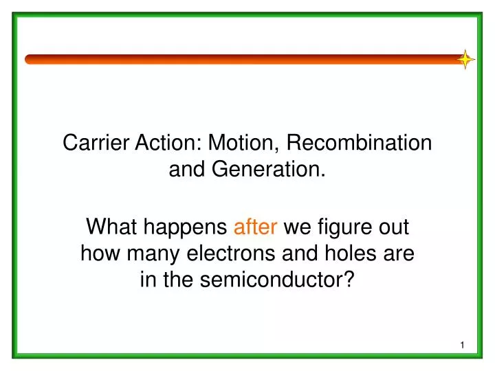
Carrier Action: Motion, Recombination and Generation. What happens after we figure out how many electrons and holes are in the semiconductor?. Described by 2 concepts: Conductivity: s (or resistivity: r = 1/s ) Mobility: m Zero Field movement: Random – over all e -

E N D
Carrier Action: Motion, Recombination and Generation. What happens after we figure out how many electrons and holes are in the semiconductor?
Described by 2 concepts: Conductivity: s (or resistivity: r = 1/s) Mobility: m Zero Field movement: Random – over all e- Thermal – Energy Distribution. Motion Electrons are scattered by impurities, defects etc. Carrier Motion I What happens when you apply a force?
Carrier Motion II • Apply a force: • Electrons accelerate: -n0qEx=dpx/dt {from F=ma=d(mv)/dt} • Electrons decelerate too. • Approximated as a viscous damping force • (much like wind on your hand when driving) • dpx = -px dt/t {dt = time since last “randomizing collision” and t = mean free time between randomizing collisions.} • Net result: deceration = dpx/dt = -px/t
Carrier Motion III • Acceleration=Deceleration in steady state. • dpx/dt(accel) + dpx/dt(decel) = 0 • -n0qEx - px/t = 0. • Algebra: • px/n0 = -qtEx = <px> • But • <px> = mn*<vx> Therefore: Mobility!
Currents • “Current density” (J) is just the amount of charge passing through a unit area per unit time. • Jx = (-q)(n0)<vx> in C/(s m2) or A/m2 = +(qn0mn)Ex for e-’s acting alone. = sn Ex (defining e- conductivity) • If both electrons and holes are present:
Current, Resistance • How do we find: • current (I)? We integrate J. • resistance (R)? • Provided r, w, t are all constants along the x-axis. E x t L V w
Mobility changes … • Although it is far too simplistic we use: mn = qt/mn* • t depends upon: • # of scatter centers (impurities, defects etc.) • More doping => lower mobility (see Fig. in books) • More defects (worse crystal) => smaller mobility too. • The lattice temperature (vibrations) • Increased temp => more lattice movement => more scattering => • smaller t and smaller m. t is the “mean free time.” mn* is the “effective mass.” (depends on material) m Increasing Doping
Mobility Changes II • Mobility is also a function of the electric field strength (Ex) when Ex becomes large. (This leads to an effect called “velocity saturation.”) Here m is constant (low fields). Note constant m => linear plot. <vx> Vsat 107 cm/s At ~107 cm/s, the carrier KE becomes the same order of magnitude as kBT. Therefore: added energy tends to warm up the lattice rather than speed up the carrier from here on out. The velocity becomes constant, it “saturates.” 106 cm/s electrons holes 105 cm/s Ex (V/cm) 102 103 104 105 106
What does Ex do to our Energy Band Diagram? • Drift currents depend upon the electric field. What does an electric field do to our energy band diagrams? • It “bends” them or causes slope in EC, EV and Ei. We can show this. • Note: • Eelectron = Total E • = PE + KE • How much is PE vs. KE??? Eelectron e- EC Eg EV h+
Energy Band Diagrams in electric fields • EC is the lower edge for potential energy (the energy required to break an electron out of a bonding state.) • Everything above EC is KE then. • PE always has to have a reference! We’ll choose one arbitrarily for the moment. (EREF = Constant) • Then PE = EC-EREF • We also know: PE=-qV Eelectron e- KE EC= PE Eg EV= PE PE KE h+ EREF
Energy Band Diagrams in electric fields II • Electric fields and voltages are related by: E = -ÑV (or in 1-D E=-dV/dx) • So: PE = EC-EREF = -qV or V = -(EC-EREF)/q • Ex = -dV/dx = -d/dx{-(EC-EREF)/q} or Ex = +(1/q) dEC/dx
Energy Band Diagrams in electric fields III • The Electric Field always points into the rise in the Conduction Band, EC. • What about the Fermi level? What happens to it due to the Electric Field? Eelectron Ex EC Ei EV Eg EREF
Another Fermi-Level Definition • The Fermi level is a measure of the average energy or “electro-chemical potential energy” of the particles in the semiconductor. THEREFORE: • The FERMI ENERGY has to be a constant value at equilibrium. It can not have any slope (gradients) or discontinuities at all. The Fermi level is our real-life EREF!
Let’s examine this constant EF + V - • Note: If current flows => it is not equilibrium and EF must be changing. • In this picture, we have no connections. Therefore I=0 and it is still equilibrium! • Brings us to a good question: • If electrons and holes are moved by Ex, how can there be NO CURRENT here??? Won’t Ex move the electrons => current? • The answer lies in the concept of “Diffusion”. Next… Semiconductor Ex Eelectron Ex EC Ei EF EV Looks P-type Looks N-type
Diffusion I • Examples: • Perfume, • Heater in the corner (neglecting convection), • blue dye in the toilet bowl. • What causes the motion of these particles? • Random thermal motion coupled with a density gradient. ( Slope in concentration.)
Green dye in a fishbowl … • If you placed green dye in a fishbowl, right in the center, then let it diffuse, you would see it spread out in time until it was evenly spread throughout the whole bowl. This can be modeled using the simple-minded motion described in the figure below. L-bar is the “mean (average) free path between collisions” and t the mean free time. Each time a particle collides, it’s new direction is randomly determined. Consequently, half continue going forward and half go backwards. 32 Dye Concentration 16 16 8 8 8 8 4 8 8 4 4 4 x -3 -2 -1 0 1 2 3
Diffusion II • Over a large scale, this would look more like: t=0 t1 Let’s look more in depth at this section of the curve. t2 t3 tequilibrium
Diffusion III • What kind of a particle movement does Random Thermal motion (and a concentration gradient) cause? n(x) It causes net motion from large concentration regions to small concentration regions. nb0 nb1 nb2 Bin (0) Bin (1) Bin (2) Line with slope: Half of e- go left half go right. x-axis
Diffusion IV • Net number of electrons crossing x0 is: • Number going right: 0.5*nb1*ℓ*A • Minus Number going left: 0.5*nb2*ℓ*A • Net is = 0.5*ℓ*A*(nb1-nb2) • (note ℓ*A=volume of a bin.) • Flux = # of particles crossing a plane per unit time and unit area. Symbol is: f f = 0.5*ℓ*A*(nb1-nb2) (t = mean free time.) t*A Or f = 0.5*ℓ (nb1-nb2) t
Diffusion V • Using the fact that slope (dn/dx) = -(nb1-nb2)/ℓ gives: f = - 0.5*ℓ2dn or f = -Dn*dn/dx (electrons) t dx or f = -Dp*dp/dx (holes) • Now: When charges move we get current. Consequently, the current density is directly related to the particle flux. The equations are: • (electrons) (holes)
Diffusion VI • Let’s look at an example: dn/dx = 0 here n(x) x J(x) x The electrons are diffusing out of the center and toward the edges.
Currents round-up • So now we know that our total currents have 2 components: • DRIFT – due to any electric field we apply • DIFFUSION – due to any (dp/dx, dn/dx) we apply and thermal motion.
Answering that old question + V - • How can we have an electric Field and still have no current? (Still have J = 0?) • Diffusion must balance Drift! Example: Semiconductor Ex Eelectron Ex EC Ei EF EV Looks P-type Looks N-type
Einstein Relationship • We next remember: p=niexp((Ei-EF)/kBT) • Plugging this into our equation for the electric field and noting that dEF/dx = 0 … we get • The Einstein Relationships. • These are very useful. You will never find a table for both Dp and mp as a result of these. Once you have m, you have D too, by this relationship.
Pretend we have: What will be the fluxes and currents? A sanity check x Holes Mechanism Electrons Ex Diffusion Flux (f) Current Density (J) Drift Flux (f) Current Density (J) n(x) p(x)
Generation (G): How e- and h+ are produced or created. Recombination (R): How e- and h+ are destroyed or removed At equilibrium: r = g and since the generation rate is set by the temperature, we write it as: r = gthermal The concepts are visually seen in the energy band diagram below. Recombination – Generation I Ee R G EC hv hv EV x
Recombination must depend upon the # of electrons: no the # of holes: po (If no e- or h+, nothing can recombine!) From the chemical reaction e- + h+ → Nothing we can know that r = αrnopo = αrni2 = gthermal When the temperature is raised gthermal increases Therefore ni must increase too! Recombination – Generation II The recombination “rate coefficient”
A variety of recombination mechanisms exist: Recombination – Generation III Ee Direct, Band to Band Auger R G EC Ee R G hv hv EC EV x Ee EV Indirect via R-G centers x R G EC R-G Center Energy Level EV x
GaAs band structure produced by J. R. Chelikowsky and M. L. Cohen, Phys. Rev. B 14, 556 (1976)using an empirical Pseudo-potential method see also: Cohen and Bergstrasser, Phys. Rev. 141, 789 (1966). GaAs is a Direct Band Gap Semiconductor Eg – The Band Gap Energy Direct recombination of electrons with holes occurs. The electrons fall from the bottom of the CB to the VB by giving off a photon!
GaAs band structure produced by W. R. Frensley, Professor of EE @ UTD using an empirical Pseudo-potential method see also: Cohen and Bergstrasser, Phys. Rev. 141, 789 (1966).
Silicon band structure produced by J. R. Chelikowsky and M. L. Cohen, Phys. Rev. B 14, 556 (1976)using an empirical Pseudo-potential method see also: Cohen and Bergstrasser, Phys. Rev. 141, 789 (1966). Si is an Indirect Band Gap Semiconductor Eg – The Band Gap Energy Only indirect recombination of electrons with holes occurs. The electrons fall from the bottom of the CB into an R-G center and from the R-G center to the VB. No photon!
Silicon band structure produced by W. R. Frensley, Professor of EE @ UTD using an empirical Pseudo-potential method see also: Cohen and Bergstrasser, Phys. Rev. 141, 789 (1966).