Download
1 / 32
320 likes | 624 Views
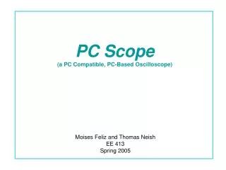
Aztec PC Oscilloscope. Michael Mason Jed Brown Josh Price Andrew Youngs. Changes in Design since PRD. Spartan 3 Starter kit replaces Spartan 3E Kit Reason: Cheaper and more readily available. Better alternative for low-income students. Not hard to tweak code for the 3E. Siemens 8051

E N D
Aztec PC Oscilloscope Michael Mason Jed Brown Josh Price Andrew Youngs
Changes in Design since PRD • Spartan 3 Starter kit replaces Spartan 3E Kit • Reason: Cheaper and more readily available. Better alternative for low-income students. Not hard to tweak code for the 3E. • Siemens 8051 • Reason: Already known by us, provides enough. • PC Communication Serial and USB • Initially PC->Scope communication will be via serial cable to the uC. • Scope Data -> PC will de via serial/USB interface from the FPGA.
Block Diagram Scope Serial M C SD R A M S C PC A/D USBController Spartan-3 eeprom
USB Controller • UM232R • UART Interface supports 7/8 bit data, 1/2 stop bits, and Odd/Even/Mark/Space/No Parity • Transfer Data Rate 300k to 1Mega Baud (RS232) • FIFO receive and transmit buffers for high data throughput. • Integrated 3.3V level converter for USB I/O.
Spartan-3 FPGA Board • Xilinx Devices: • Spartan-3 (XC3S200) • Clocks: 50 MHz crystal clock oscillator • Memory • 256Kx16 ISSI - 10 ns SRAM devices
Spartan-3 Starter Kit • Connectors and Interfaces • Xilinx Spartan-3 FPGA w/ twelve 18-bit multipliers, 216Kbits of block RAM, and up to 500MHz internal clock speeds • -200, -400, and -1000 versions available • On-board 2Mbit Platform Flash (XCF02S) • 8 slide switches, 4 pushbuttons, 9 LEDs, and 4-digit seven-segment display • Serial port, VGA port, and PS/2 mouse/keyboard port • Three 40-pin expansion connectors • Three high-current voltage regulators (3.3V, 2.5V, and 1.2V) • 1Mbyte on-board 10ns SRAM (256Kb x 32)
Microcontroller • Siemens 8051 • 16-bit addressable, 8-bit data, 64kB accessible external RAM • Basic control unit for enables, external peripherals (SPI with ADC) • Will interface with the computer for sending data and receiving user commands (RS-232).
Latch, Decoder, EPROM, and SRAM from uC(32kx8 EPROM for program memory) (32kx8 SRAM for external memory)
Serial Peripheral Interfacing (SPI) • SCK (Serial Data Clock): Data is shifted/latched on the rising or falling edge of SCK (see next section). • MOSI (Master Output/Slave Input): Data is transmitted out of this pin if the chip is a Master and into this pin if the chip is a Slave. • CS (Chip Select, active low): Tells the peripheral that a transfer is about to begin.
Analog to Digital Conversion • Differential Input • ADC: 3V peak to peak maximum input • Voltage Reference
Input Stage • Capacitive Impedance matching • 1:1, 10:1 Attenuation • AC Coupling
Feedback Control 4 Gain Levels: 2, 4, 6, 10
Gain Stage #2 • CLC5526: Digitally Controlled Variable Gain Amplifier • +30 dB to –12dB
ADS807 • Internal Reference Voltage • Input: 3Vpp (V+ - V- <3V) • Clock Input from FPGA: 10k to 53M samples/sec • 12-bit Output Buffered, sent to FPGA
Software – FPGA • Labview Module using VESA interface. • Communication via virtual COM port drivers. • Cause the USB device to appear as an addition com port available to the PC. • Applications can access the USB device in the same way as it would access a standard COM port.
Software – User GUI • Initial development in both MATLAB and Labview • Labview has better interface modules but more difficult to program the GUI. • MATLAB is easier to program the GUI but the advanced controls will be more difficult • Use Labview to develop GUI with MATLAB as a fallback.
Graphical User Interface • Inputs • Data will be inputted via USB from the FPGA board. • Data Format • 8 bit data transfer • 1 stop bit • 0 parity bits • Data speeds will be 300k – 1M baud
Graphical User Interface - cont. • Outputs • Serial output to Microcontroller • Data will be 8 bit with 1 stop bit. (RS232) • Graphical Output to Monitor • Data Graphs • Controls to manipulate data graph and perform analysis. • Control inputs to be sent to micro controller.
Timeline – Milestone 1 • Micro controller • Programming Complete • Serial Interface Working • A/D Converter • Circuit design complete • Prototype complete and tested • FPGA • Programming mostly complete • USB interface started • Software • GUI preliminary programming, simple I/O • PCB • Schematics completed for 1st revision.
Timeline – Milestone 2 • FPGA • Programming complete • Trigger mode enabled • Software • GUI updated to include all necessary functionality. • PCB 2 • 2nd Revision submitted and received. • Make sure PCB is working • A/D • Filtering implemented as necessary
Timeline – Expo • Scope Working • All parts integrated • PCB completely tested and connected to FPGA board. • Extras • GUI interface updated as time allows • Documentation Completed • USB interface working • Data transmitting from FPGA to PC • GUI • Sending signals to micro controller • Updated graphing capabilities • PCB • 2nd revision submitted and tested. • A/D connection to FPGA • Data being received and stored
Division of Labor • Mike • Software – GUI Interface, FPGA Programming • USB Interface • Assist Josh with microcontroller and Drew with A/D • Jed • FPGA Programming • Software Interface • Assist with A/D converter • Drew • A/D converter • Microcontroller Interface • FPGA Interface • Josh • Microcontroller • Interface with A/D converter • Serial Interface with Computer