Download
1 / 27
270 likes | 277 Views
PCB design with Design E ntry CIS and Layout Plus. ECE-121 TA: Ritu Bajpai. Drawing the schematic. We have a new version of cadence in the lab now. You will find it listed under ALL PROGRAMS as cadence 16.1 (I am not sure if 16.1 but 16 something)

E N D
PCB design with Design Entry CIS and Layout Plus ECE-121 TA: Ritu Bajpai
Drawing the schematic • We have a new version of cadence in the lab now. You will find it listed under ALL PROGRAMSas cadence 16.1 (I am not sure if 16.1 but 16 something) • We will use design entry CIS to make the schematic • If given an option you will choose PCB design allegro in the beginning • Start a new project as we used to do in the older version
Drawing the schematic Click this icon to bring up the place part window Click this icon to add libraries
Libraries • You can pick up your components from the following libraries • Diode from Pspice-diodes • TIP 31A and TIP32A from Pspice-pwrbjt • Voltage regulator and LM741 form Pspice-Opamp • Resistors and capacitors from Pspice-analog Note: You will not find your diode number in the diode library. You can use any other diode because we only need to select the right foot print. More on this later in the slide show.
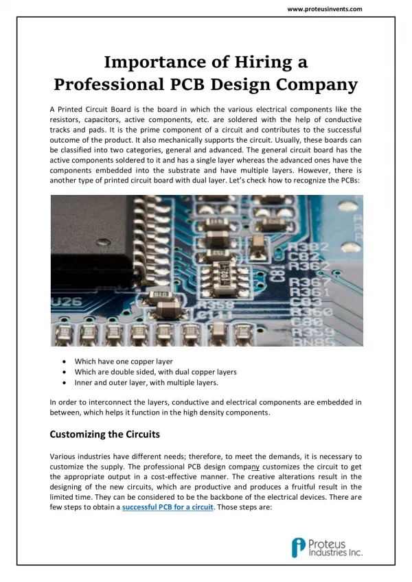
PCB design • The PCB board that we will build is the simplest type with insulating layer in between two conducting layers of Cu on top and bottom • Since our aim is to export the design to layout plus and create a layout for our PCB board, we are not concerned with the values of the components. You can leave them as default values. • Do not connect a AC source as an input to the voltage rectifier.
In place of the AC source we want two vias where we should be able to provide transformer connections. • A via is a through hole in the PCB • We could connect a resistor across the two points where the AC power supply to the rectifier is connected • This will generate 2 vias where we will be able to connect power supply from the transformer
Matching the pins • Once you have connected all the components, recheck your circuit because once the PCB is made you cannot change your connections. • Match the pin numbers on the schematic with the pin numbers of the parts in your kit. • For example, TIP BJTs have pins 1,2 and 3 as the base, collector and emitter for the component in your kit. The numbers should correspond to the same in the schematic.
Matching the pins • Can you find any component for which the pin numbers don’t match? • LM7805 has pins 1 input, 2 gnd and 3 output on the part in your kit but in the schematic it has 1 input, 2 output and 3 gnd • This will swap pins 2 and 3 for us when we put the component on the board • So we will create our own symbol for LM 7805 and give it the pin numbering that we want
New library You can save your library with a new name if you like
Creating a part Select library name and right click to get the menu and then click New Part
Creating a part You can name your part LM7805C and PCB Footprint as TO220. Click OK
Creating a part Use “draw line” from the tool bar on the right to draw a box along the dotted line. Next use pin icon from the toolbar to draw pins. Name them IN, GND and OUT and number them 1,2 and 3 respectively. Type will be input, power and output respectively.
Creating a part • Having created the part, you can remove the LM7805 symbol that you had used from opamp library and replace it by the symbol that you just created. • Now you are ready to create a Netlist for your design. • Before that you will have to modify the footprint name for some of the components as this software will not accept / and . in the footprint name. This is just a software compatibility problem. • We will modify the footprint name for the resistors, capacitor and LM 741
Modifying footprint name • Select a resistor • Right click and choose edit properties • Scroll to the right to find part footprint • Note the value of the footprint as you will need it later • Now modify the footprint name to remove any . or / in the name • Do this for all the resistors, capacitors and LM741
Creating the netlist Click on schematic, then go to Tools and click on create netlist. Create netlist window pops up, hit OK. This should create a .MNL file in your project folder. Sometimes it doesn’t show the .MNL file immediately in which case try creating the netlist again.
Starting Layout Plus • Now we will start the layout plus software again from cadence 16 • Go to file->New • For input Layout TCH browse the file default.tch (not _default.tch) • For input MNL file read your netlist file from your project folder • Hit apply ECO.
Select footprint • You will now need to link your components to the footprints. • The software will automatically read some footprints but not all so you will have to enter the ones that it does not take on its own. • We will use 1st option of linking existing footprint to component
Footprints • Footprints basically contain the information about physical dimensions and distances between pins of the device so that vias for placing the component on the PCB can be made accordingly. • For your design look for the footprints LM 741 will be in DIP100 LM7805 will be in TO, look for TO 220 showing pins 1,2 and 3 Capacitor, Resistor and Diode footprints are in the libraries TM_CAP_P, TM_AXIAL and TM_DIODE respectively. Use the footprint names that you earlier made a note of. For diode use DO35
After choosing all the footprints you will get a view of all your components • Place the footprint within the rectangular outline. • Place the design components so that they are evenly spread out. This will make routing and tracking easier later on.
Settings • Select View Spreadsheet in the toolbar (A grid like icon). A pop-up menu will appear. • Select Nets. The Nets spreadsheet will appear. • Select the "Width" cell. All the cells in that column should be highlighted. • Right click the mouse and select Properties from the pop-up menu. The Edit Net dialog box will appear. • Change Min Width to track width 30 (mils). Change Conn Width to 50 (mils). Change Max Width to 65 (mils). Click O.K.
Settings • Next ensure the pad widths are 80mils. • Select View Spreadsheet in the toolbar. A pop-up menu will appear. • Select Padstacks. The Padstacks spreadsheet will appear. • Select the Pad Width and Pad Height cells. Right-click and select Properties. • Enter 80 (mils) for both Pad Width and Pad Height. Click O.K.
Settings • Next disable all layers for routing except the BOTTOM. Select View Spreadsheet in the toolbar. Select Layers. • In the Layers spreadsheet, click on the Layer Type cell to highlight the entire column. Press the Ctrl (on the keyboard) and click the BOTTOM. • Right-click and select Properties. In the Edit Layer dialog box, select the Unused Routing option. • Now all tracks will be routed on the bottom layer. This will simplify component soldering once the board is fabricated.
Drawing the board outline • Click on the Obstacle Tool in the toolbar. • Place the crosshair of cursor on the black field of the design window and double click. • The Edit Obstacle window should appear. • Select Board Outline for the Obstacle Type. • Change the Width to 62 mils. • Select Global Layer for the Obstacle Layer. Click OK. • Begin drawing enclosed border of the design.
Select Auto-> Autoroute -> Board. The software will route the board. • When it is done, a pop-up window will announce that the task has been completed. Click O.K. • Any thin yellow connections still present in the layout show that those tracks have not been routed. • Select Auto->Unroute->Board. Move the components around and try routing it again. • Its more of a hit and trial thing but if you are not able to route it, you can enable both top and bottom layer for routing.
Creating Gerber files • Once done with routing proceed to creating Gerber files • Step by step instructions are on the lab website