Download
1 / 12
130 likes | 255 Views
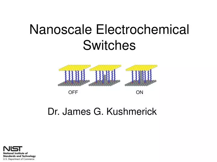
Nanoscale Electrochemical Switches. Dr. James G. Kushmerick. OFF. ON. Nanoscale Electrochemical Switches. ~ 2 nm. OFF. ON. 1. OFF state – molecular tunnel junction 2. V threshold reached. Ag + filament bridges gap. Switches ON. 3. Remains in ON state until polarity switched.

E N D
Nanoscale Electrochemical Switches Dr. James G. Kushmerick OFF ON
Nanoscale Electrochemical Switches ~ 2 nm OFF ON 1. OFF state – molecular tunnel junction 2. Vthreshold reached. Ag+ filament bridges gap. Switches ON. 3. Remains in ON state until polarity switched. 4. At 0 V, device is returned to OFF state. Device can be rapidly cycled between ON and OFF Greater than 1 million switch cycles achieved Fastest monolayer switch to date = 13 kHz On-Off Ratio > 105 Device area ~ 25 nm2
10 1.0 Minimum Feature Size (mm) 0.1 0.01 1970 1980 1990 2000 2010 2020 CMOS Scaling 65 nm node (2005) …drives Si technology towards fundamental limits Courtesy of Intel Rock’s Law: the cost of a semiconductor chip fabrication plant doubles every four years Courtesy INTEL
Nanoscale Crossbar Fabrication Science 300 (2003) 112-115
Advantages • Ease of fabrication • Huge On-Off Ratio (>105) • High success rate for device fabrication (>90%) • Small Device Area (~25 nm2) Challenges/Opportunities • Slow Switch Speed (~10 kHz) defines possible applications (e.g. memory arrays and FPGA) • Not easily integrated into CMOS fab-line, but no fab-line needed
Technology Applications • Nanoscale Electrical Devices • Memory Arrays • Field-Programmable Gate Arrays Commercial Applications • Memory and logic for cell phone and other portable electronic devices
Future Work • Optimization of switch characteristics • Increase switch speed • Increase # of cycles till failure • Fabricate nanoscale memory devices
Collaboration Opportunities • Future work would best be done in collaboration between NIST and an interested industrial partner. • Intellectual Property: “Self-Assembled Monolayer Based Silver Switches ” Provisional Patent Application filed 9/10/2007 Serial # 11/852,811
Contact Information • For further information contact: • James G. Kushmerick100 Bureau Drive Stop 8372Gaithersburg, MD 20899-8372Tel: (301) 975-5697email: james.kushmerick@nist.gov