Download
1 / 9
100 likes | 365 Views
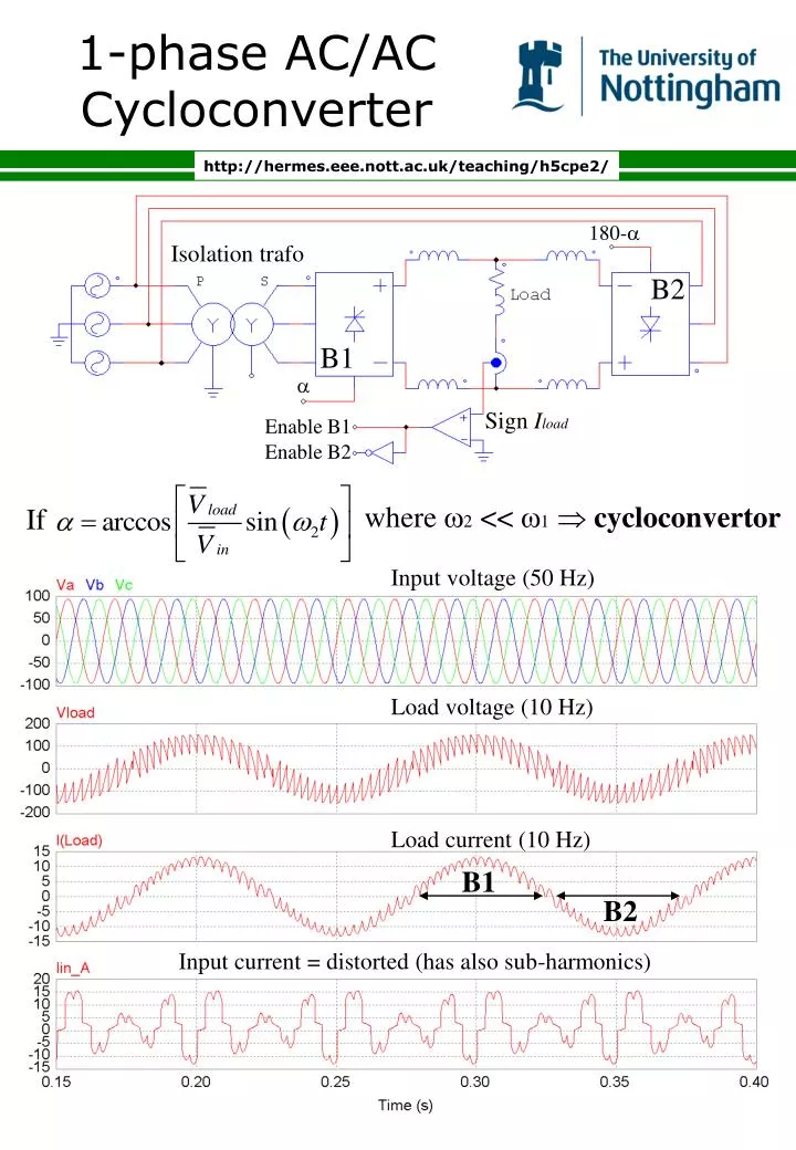
1-phase AC/AC Cycloconverter. 180-. Isolation trafo. B2. B1. . Sign I load. Enable B1. Enable B2. http://hermes.eee.nott.ac.uk/teaching/h5cpe2/. where 2 << 1 cycloconvertor. If . Input voltage (50 Hz) . Load voltage (10 Hz) . Load current (10 Hz) . B1. B2.

E N D
1-phase AC/AC Cycloconverter 180- Isolation trafo B2 B1 Sign Iload Enable B1 Enable B2 http://hermes.eee.nott.ac.uk/teaching/h5cpe2/ where 2 << 1 cycloconvertor If Input voltage (50 Hz) Load voltage (10 Hz) Load current (10 Hz) B1 B2 Input current = distorted (has also sub-harmonics)
Classification of PWM Converters http://hermes.eee.nott.ac.uk/teaching/h5cpe2/ Voltage Source Inverter Current Source Inverter Inductive load Capacitive (voltage Source) dc-link Inductive (Current Source) dc-link Capacitive load Voltage Source Converter (rectifier+inverter) Cdc Vdc=unipolar Current Source Converter (rectifier+inverter) Ldc Idc=unipolar
DC-link Voltage Comp. in PWM-VSI 6 V http://hermes.eee.nott.ac.uk/teaching/h5cpe2/ Ldc/2 3-ph Voltage Supply 3-ph R-L Load Cdc 3-ph Diode Rectifier Ldc/2 3-ph PWM Voltage Source Inverter L-C smoothing=based on energy storage components • Small dc-link voltage ripple still present (no filter is perfect!!) • The 6 V ripple compared to 550 V mean value (1%) causes no visible impact on output voltage& current waveform • What would be the effect of reducing the filter size (cost)?
DC-link Voltage Comp. in PWM-VSI http://hermes.eee.nott.ac.uk/teaching/h5cpe2/ Reduced dc-link capacitor size Vdc = 70 V 70 V No dc-link capacitor Vdc = 80 V 80 V No dc-link capacitor still able to operate !!
DC-link Voltage Comp. in PWM-VSI Modulating fnc Vout dutycycle = * Vpk-carrier Vdc No dc-link capacitor Vdc = 80 V 80 V http://hermes.eee.nott.ac.uk/teaching/h5cpe2/ H-bridge output voltage = Vdc*(2*dutycycle - 1) Vdc&Vout = linear dependency: Vdc ripple Vout distortion compensation Vdc ripple no visible distortion in output waveforms 120 Input current=typical diode rectifier with Id=const (current source rectifier)
Direct Power Converters http://hermes.eee.nott.ac.uk/teaching/h5cpe2/ Bidirectional switches on input side give the possibility to commutate the dc-link current to the input line of choice: increase conduction angle from 120 to 180 degrees and shape the average input currentsinus It is possible to combine the functionality of rectifier stage switches and inverter stage switches MATRIX CONVERTER Virtual Single Stage AC/AC converter with no dc-link storage, sine wave input current sine wave output voltage capability Problems: many semiconductor devices, Vout = 86% Vin, sensitive to input voltage disturbances
Matrix Converter: Bidirectional switch Diode embedded switch: - 4 FRD and 1 IGBT - higher conduction losses (2 FRD and 1 IGBT) - higher switching losses (hard-switching) Overlap comm. Dead time comm. Ideal comm. a) SA SB Anti-paralleled switch: - 2 FRD and 2 IGBT - lower conduction losses (1 FRD and 1 IGBT) - lower switching losses (semi-soft switching) - Common Emitter (CE) connected (b) - Common Collector (CC) connected (c) - Anti-paralleled Reverse Blocking IGBTs b) SA A VA ~ c) out VAB SB Bidirectional Switch Commutation: VB ~ Iout Zload B on on on off off off on on on off off off http://hermes.eee.nott.ac.uk/teaching/h5cpe2/
Matrix Converter: Bidirectional switch State diagram of IGBTs A(+) B(-) 11 - 00 Iout >0 Iout <0 Gate Driver 01 - 00 10 - 00 01 - 01 10 - 10 00 - 01 00 - 10 IL >0 ULine >0 00 - 11 SAp SAn Switch format symbol: ON ON SA - SB SBp SBn ApAn–BpBn OFF OFF http://hermes.eee.nott.ac.uk/teaching/h5cpe2/ Load current sign controlled commutation • Better measure currents than voltages • Suitable for 3/1 phase modular approach • Inductive currents give a more stable sign signal • Failure in detecting the correct sign causes dead-time commutation (Li2 = small if offset)
Performance of a Matrix Converter Uin Iin Imot Umot Uin Iin Imot Uin Iin here the DC-machine starts motoring IDCgen http://hermes.eee.nott.ac.uk/teaching/h5cpe2/