Download
1 / 23
230 likes | 369 Views
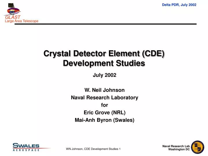
Crystal Detector Element (CDE) Development Studies. July 2002 W. Neil Johnson Naval Research Laboratory for Eric Grove (NRL) Mai-Anh Byron (Swales). Fabrication processes for CDE have been studied at NRL and selected for EM fabrication.

E N D
Crystal Detector Element (CDE)Development Studies July 2002 W. Neil Johnson Naval Research Laboratory for Eric Grove (NRL) Mai-Anh Byron (Swales) Naval Research LabWashington DC
Fabrication processes for CDE have been studied at NRL and selected for EM fabrication. CDE = wrapped Csl Crystal bonded with photodiode ass’y (PDA) at each end. Processes defined since PDR Bonding of PDA to CsI xtal CTE mismatch between PDA and xtal causes stress in bond Hard epoxies fail, silicones (without primer) don’t adhere Need soft, flexible bond with strong adhesion Solution: Silicone elastomer with primer. Bond laid up in mold that defines geometry. Wrapping of xtal Material is 3M VM2000 non-metallic, specular, reflective film High light yield, good optical properties Material is stiff, difficult to fold or wrap Solution: Mold in mandrel at 120C for 2 hrs at final shape CDE Development Dual PIN photodiode with flex cable = photodiode assembly Naval Research LabWashington DC
Scope of Bonding Studies • Assumptions • The bond shall be made with DC93-500 silicone encapsulant, with DC92-023 primer applied to all bonding surfaces. • The bond thickness shall be 0.7 0.1 mm. • The bond material shall not extend past the edges of the diode, lest it interfere with the bumper. • The crystal surface shall be roughened to improve adhesion. • Parameters studied • Method of bond lay-up • Selected one-stage mold with mask to define bond geometry • Encapsulant is injected into bounded volume • Mix ratio of DC93-500 encapsulant • Conclusion: vendor-recommended 10:1 is soft enough after cure • Amount and method of DC92-023 primer to be applied • Conclusion: measured volume of primer is spread with spatula • Surface treatment of diode and xtal (factory polish or roughened) • Conclusion: diode to remain polished, xtal to be roughened Naval Research LabWashington DC
Bonding Methods Studied • Four bonding methods studied at NRL and Swales • “Spacer” method (at NRL). • Deliver measured amount of 93-500 between diode and xtal held fixed distance apart. • OK, but susceptible to measurement errors. Rejected. • “Two-stage” method (at NRL). • Create pad of 93-500 on diode face, cure for one day, wet surface of 93-500 and apply to xtal. • OK, but susceptible to incomplete curing. Rejected. • “Two-stage” method (at Swales). • Similar to NRL version, but uses more 93-500 in 2nd stage and more precise volume. • OK, but complex. Rejected. • “One-stage” method (at Swales). • Form bond within break-apart Teflon mold holding diode and xtal. • Makes very strong and precise bonds. Selected. Naval Research LabWashington DC
Bonding Method Selected • One-stage mold • Principles of method • Bond is formed within break-apart Teflon mold holding diode and xtal • Mold precisely defines bond thickness, area, and location on face of xtal • Mold is sealed against xtal face to prevent leakage of silicone encapsulant • Encapsulant is injected into bond cavity and allowed to flow until any trapped bubbles are removed • Bonding procedure is written and configured • “Process Specification for the Bonding of the PIN Photodiode Subassembly to the CsI Crystals", LAT-PS-00385-01 Naval Research LabWashington DC
Bonding fixtures • Exploded view of PDA and Mold subassembly • Mold: defines location of bond on xtal (referenced to xtal corner) • Mask: defines bond thickness (0.7 mm) and area (covers epoxy resin) • Seal and O-rings: prevent spread of encapsulant outside bond area Mask Seal Photodiode Assembly Mold O-Rings Photodiode Assembly Mask Xtal Bond Naval Research LabWashington DC
Bonding fixtures • Fixture and molds for single crystal • Independent bonding molds are created for each crystal end • Support sleeve prevents distortion of crystal and registers mold to corner of crystal Support Fixture CsI(Tl) Crystal Mold and PDA Subassembly Flex Cable soldered to Photodiode Naval Research LabWashington DC
Bonding fixtures • Bonding work station • 12 bonding stations, six on each side • Encapsulant is injected with CDE in vertical position Worktable Injection syringe for DC93-500 Injection performed at this face. Cure for 24 hours before flipping 180° to bond opposite face. Crystal Bond Set-Up Assy.6 mounted on near side6 mounted on far side Naval Research LabWashington DC
Bond Process • Process at Swales Aerospace • Prepare Surfaces • Clean factory-polished diode bond surface • Clean roughened crystal surface • Allow cleaned surfaces to air dry • Position Crystal into Fixture and Prime • Position xtal into fixture • Adjust pads to align xtal into proper position • Prime xtal surface with DC92-023 • Position Photodiode into Mold and Prime • Assemble diode into mold cavity • Create desired bond area by assembling mask to mold assembly • Prime diode surface with DC92-023 Inlet & Outlet Holes Figure 1: Diode in Mold, Top Side of Mold Diode in Cavity Mask in Cavity Figure 2: Diode & Mask in Mold, Back Side of Mold Naval Research LabWashington DC
Bond Process (cont.) • Join Mold and Xtal fixture • Assemble fixture (which now contains crystal) to mold assembly • Preload crystal to mask/diode surface to create a tight seal • Apply Adhesive • Prepare adhesive mixture and de-gas • Slowly pour mixed/degassed adhesive into syringe • Inject adhesive into mold inlet hole until the bond cavity is filled • After Injection • Wipe clean adhesive from areas around inlet and outlet hole • Cure for 24 hours until tack free • Remove bonded crystal & diode from mold after 24 hours • Allow bond to finish 7-day cure Naval Research LabWashington DC
Mechanical Test Sample Bonds (All Bonds Displayed No Bubbles & Desired Bond Profile (Area & Thickness; Bond Maintained in Ceramic Frame ) Figure 13: EM Diode on Xtal, Side View Figure 14: EM Diode on Xtal, Front View Figure 15: EM Diode on Xtal, Back View Figure 16: EM Diode on Xtal, Side View Figure 16: EM Diode on Xtal, Side View Figure 17: EM Diode on Xtal, Front View Figure 18: EM Diode on Xtal, Back View Figure 19: EM Diode on Plexiglas, Back View Naval Research LabWashington DC
Light Yield • Light yield tests were performed on sample xtals 3 x 3 x 19 cm • Requirement on CDE • >6000 e/MeV in large PIN photodiode • Tests were performed on sample xtals • Xtal size = 3 x 3 x 19 cm • EM photodiode • Tetratex wrap • Samples exposed to radioactive source with known line energy • Measured yield (after 50 thermal cycles) • 6200 – 7000 e/MeV • Expect yield of >7500 e/MeV for EM dimensions with VM2000 wrap Naval Research LabWashington DC
Thermal Cycling • Bonds need to be mechanically strong and maintain optical properties • To survive handling loads • To survive thermal cycling in test, shipping, and storage • How do we know a bond has survived? • A bond can be mechanically strong and show no visual evidence of separation, at the same time that it has optically failed! • Bond process qualification plan must include readout of scintillation light. • Visual inspection is inadequate and unacceptable as proof of bond quality. • Thermal cycling • Full qualification range: –30C to +50C • Gradient: 20C per hour (if much steeper, xtals can’t keep up) • Soak: 1 hour at –30C, 1 hour at +50C • Irradiate xtal sample with 137Cs, monitor 662 keV centroid after series of thermal cycles Naval Research LabWashington DC
Thermal Cycling • Optical performance of test samples under thermal cycling • Test samples are 3 x 3 x 3 cm cubes with single EM photodiode • Test samples typically decline ~5% from their initial light yields and reach plateau • Expect this to translate to ~10% decline in CDEs • Optical properties ofbonds survive thermalcycling • Bonding processcreates thermallystable bonds Naval Research LabWashington DC
Thermal Cycling • Optical performance of longer xtal samples • Longer xtals samples are 3 x 3 x 19 cm with EM diodes on both ends • Typically decline ~10% from initial light yield • Expect same performance from CDEs • Again, bondingprocess createsthermally stablebonds • Adhesion problemis solved Naval Research LabWashington DC
Early Thermal Cycling Tests • Prior to creation of stable bonding process • 16 sample bonds • Created with several methods early in bonding study • 13 survive cycling • 3 have optical failure • Optical failures • ~15% degradation in test sample is equivalent to ~50% degradation in CDE. • We extracted samples for mechanical strength tests after optical failure… Optical failures Naval Research LabWashington DC
Xtal Xtal Mechanical Strength Tests • Two types of destructive tests have been performed at NRL • Tensile strength • CETIM requirement: 10 N (2.2 lbf) • Shear strength • CETIM requirement: 0.12 N/mm2 (8 lbf = 35 N for EM diode) • >35 samples tested • Samples are pulled or sheared to failure in Dynamic Load Test Stand Piston Piston Diode Bond Naval Research LabWashington DC
Tensile Strength Test • Swales one-stage bond • After optical failure in thermal cycling • Visual inspection showed no evidence for air gaps, delamination, separation, peeling, etc. • Subjected to tensile strength test • Bond failed at ~280 N. • Bond failed at diode face, not at xtal face. • Bond strength is >25x requirement, even after it has degraded from excellent to poor optical contact. Naval Research LabWashington DC
Shear Strength Test • Swales one-stage bond • Subjected to shear strength test • Bond failed at ~240 N. • Bond failed at diode face, not at xtal face. • >10 shear tests have been performed • Failure occurs typ. at >300 N Naval Research LabWashington DC
Crystal Wrapping (LAT-PS-00795-01) • VM2000 specular film • Gives 20-30% more light than standard diffusive white wraps (e.g. Tyvek, Tetratex) • Stable, rigid material will not wet xtal surface as Teflon-based wraps can (e.g. Tetratex) • Non-metallic, so no grounding issues • Rigid, so awkward to wrap • Tried rolling, folding, spiral winding… • All created loose, awkward wraps • Solution: Hot molding • Method • Form VM2000 around aluminum mandrel in xtal form (with chamfers) • Heat at 120 C for 2 hrs • Material takes and holds sharp corners of mandrel • Trivial to wrap around xtal, simple Kapton tape tacking • No loss in light yield or mechanical stability from hot molding Naval Research LabWashington DC
Wrapping Studies & Conclusions • VM2000 Max. Molding Temperature as Specified by 3M is 125ºC for 5 hrs. • At this temperature or any other temperature below, material properties (mechanical, physical and optical) are NOT compromised as long as material is mechanically supported. • Temperatures Studied For VM2000 Molding • 50ºC, 75ºC, 100ºC, 120ºC, 150ºC • Duration of Time for Molding Process at all Temperatures • 1 hour, 2 hrs., 3 hrs. • Conclusions: • the higher and the longer the temperature, the more defined the wrapping form • 150ºC is too high for any duration of time tested • 100ºC and 120ºC for 3 hours and 2 hours respectively is ideal • Molding VM2000 in oven allows wrap to be preformed days/weeks before actual wrapping process on real crystal has to be performed. Naval Research LabWashington DC
Wrapping Mold Set-Up Naval Research LabWashington DC
Wrap & Chamfer Close-Up Naval Research LabWashington DC