Download
1 / 34
340 likes | 479 Views
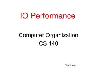
Serial IO. Tr. Serial Peripheral. MPU. Rcv. IOW. IOR. Basic concepts in serial IO. Interface requirements Address decoding, control signal generation Alphanumeric codes ASCII, EBCDIC or any other coding Transmission format Synch or asynch, simplex/duplex, rate of transmission

E N D
Tr Serial Peripheral MPU Rcv IOW IOR Basic concepts in serial IO • Interface requirements • Address decoding, control signal generation • Alphanumeric codes • ASCII, EBCDIC or any other coding • Transmission format • Synch or asynch, simplex/duplex, rate of transmission • Error checks • Parity, checksum, CRC • Data comm over telephone • Voice:300Hz-3300Hz,Modem,fsk/psk/qpsk etc
Syn and asycn transmission a) Synch format b) asynch format
Serial bit format • Baud: number of signal changes per second; bits/second. • At 1200 baud; ASCII character I (49H) is presented • 11 bits includes 1 start, 8 data and 2 stop bits • D7 can be used as parity.
Serial I/O standards • Commonly used to interface terminal, printer or modem. • Standard is a common specification that all the manufacturer have agreed upon. • Assigment of pin position for signal, voltage levels, speed, length of cables and mechanical specs. • Current loop • 20mA or 60mA, signals relatively noise free and suitable over a long distance. • voltage level • RS 232C, most commonly used method • DTE, DCE
RS 232C • Speed 20Kbaud. • Distance 50 ft. • Logic zero: +3v to +15V • Logic one: -3v to -15V • Other signals are TTL. • 25 pins
Minimum interface with RS232C • Usually printer is a DTE • Modem is a DCE
Software controlled Asycn serial I/O • Output start bit • Convert chara into serial stream with appr delay. • Add parity • Output stop bits.
rcv transmit Rd o/p port N Init bit cntr Snd strt bit Strt bit? Y Wait ½ bit time Wait bit time N Bit still low? Get chr into A Y Set bit cntr Clr data rgstr o/p bit using D0 Wait bit time Rd i/p Save bit Wait bit time Rotate nxt bit to D0. Dcr bit cntr Redy to rcv nxt bit Dcr bit cntr N Last bit? N Last bit? Y Add parity Snd stop bits Chk parity Wait for stop bits return return
D3 D4 D0 D6 D1 D2 D5 D7 SOD X SDE For interrupts 1=enable 0=disable 8085 serial I/O lines • SOD (serial output data) • SID (serial input data) MVI A, 80H ; Set D7 =1 RAR ; set D6 = 1, bring carry into D7 SIM ; output D7 D3 D4 D0 D6 D1 D2 D5 D7 SID RIM ; reads a bit and put into D7 For interrupts Serial i/p data
Data trans using SOD • Send ascii char stored in B register. SODATA: MVI C, OBH ;setup counter C to 11 bits XRA A ; reset carry to 0 NXTBIT: MVI A, 80H ; set D7 to 1 of accumltr RAR ; Bring D7 into D6 SIM ; output D7; start bit CALL BITTIM ; wait for 1 bit time STC ; set carry =1 MOV A,B ; place ASCII chr into ACC RAR ; place ascii D0 in the carry, and 1 in D7 MOV B,A ;save ACC to B DCR C ;one bit transmitted JNZ NXTBIT ; if not all bits transmitted, go back RET
(B) = 47H 0 1 0 0 0 1 1 1 CY D7 D6 D5 D4 D3 D2 D1 D0 XRA A 0 0 0 0 0 0 0 0 0 MVI A, 80H 0 1 0 0 0 0 0 0 0 RAR 0 0 1 0 0 0 0 0 0 SIM outputs 0 as stop bit STC 1 0 1 0 0 0 0 0 0 MOV A,B 1 0 1 0 0 0 1 1 1 RAR 1 1 0 1 0 0 0 1 1 MOV B,A B= 1 0 1 0 0 0 1 1 DCR C C= 0 0 0 0 1 0 1 1 JNZ NXTBIT 1 1 0 0 0 0 0 0 0 RAR 0 1 1 0 0 0 0 0 0 . When ascii D7 is sent out, register B will have all 1s from D0 to D7. In the last two iterations logic 1s are sent out as stop bits.
Data reception using SID SIDATA: RIM ; read input bit RAL ; plc D7 into CY JC SIDATA ; if D7 = 1, not a start bit, go bck and read again CALL HALFBIT ; if D7=0. strt bit. wait hafl bit time MVI C, 09 ; bit cont = 9 NXTBIT: CALL BITTIME ; wait for one bit time RIM ; read input bit RAL ; save the bit D7 to CY DCR C ; one bit read JZ RETURN ; if all bits are read return to main prog MOV A,B ; plc the bits saved so far into acc from B RAR ;plc bit saved in CY to D7 and sft all bits by 1 position MOV B,A ; save bits in B JMP NXTBIT ; get nxt bit
HW controlled serial I/O • SW control has following requirements: • An input port and an output port are req for interfacing. • In transmission, MPU converts parallel data into serial bits. • In reception, MPU converts bits from serial to parallel. • Trans and rec must match the time delay. • In HW control has serial IO, all these features are incorporated in one chip, like 8251A (USART).
8251A • Chip select • Control/Data • Write • Read • Reset • Clock • Control register • 16 bit, mode instr, command instr • Status register • It has the same add as the control register • Data buffer • bidirectional
Control logic and registers • Control regstr • 16 bit: 2 independent bytes • 1st byte: mode instr • 2nd byte command inst • Status rgstr • Chks the rdy ststs of peripheral • Accessed when C/D’ is high • Same port add as control regstr • Data buffer • Bi directional • At C/D’ is low
Blk diagram of Trn and Rcv section • Transmitter section • TxD: serial bits are tran on this line. • TxC: controls bit trans rate. Clk freq can be 1,16,64 times the baud. • TxRDY: o/p signal,high indicates the trans buffer is empty and USRT ready to accept a byte. Signal is reset when data is loaded in the buffer. • TxE: o/p signal High indicates that the O/P register is empty. Reset when a byte is trnasferd frm buffer to o/p rgstr.
Receiver section • RxD: bits are rcvd serially on this line • RxC: controls the rate at which bits are rcvd by USART. In asych mode, it can be 1, 16 or 64 times the baud. • RxRDY: it goes high when USART has a char on the input buffer register and ready to transfer it to MPU. Can be used either to indicate the status or to interrupt MPU.
Initializing 8251A • Mode, baud, stop bits, parity, etc. • Control word: a) mode word b) command word • After a reset operation, a mode word must be written in the control register followed by a command word. Command word can be changed at any time during operation, but mode can only be changed only after a reset operation. It can be reset using internal reset bit (D6) in the command word.
Interfacing RS232 terminal using 8251A • TxC is 153.6 kHz. • Asycn mode with 9600 baud • Character length = 7 bits, two stop bits • No parity check. • Port add • Data register: FEh • Control/status register: FFh
1 0 1 0 1 1 0 0 • Mode word: D7 D6 D5 D4 D3 D2 D1 D0 =CAh Baud= TxC/16=153.6k/16 = 9600 No parity Stop bits 7 bits chr • Command word (asynch mode): D7 D6 D5 D4 D3 D2 D1 D0 =11h 1 X X 0 X 1 X 0 Tr Enbl Prvnts Intrnal reset Rcv Disbl Err Rst • Status word: D7 D6 D5 D4 D3 D2 D1 D0 X X =01h X X X X 1 X Tr rdy
Initialization intruction: SETUP: MVI A, CAh ; load mode word OUT FFh ; write mode word to control rgstr MVI A, 11h ; load command word OUT FFh ; enable trnsmitter STATUS: IN FFh ; read stats word ANI 01h ; mask all bits except D0 JZ STATUS ; if D0 = 0, Tr buffer is full, go back and wait
8086/8088 Architecture • Seven categories of signals. • Max/min mode: min mode is used for single procss. Max mode is used for multiprocss • Test: synchronize multiple processors • Data Enable: generally connected to biriectional buffer to isolate MPU from system bus. • Data tran/rcvr: controls data flow. • IO or memory: indicates whether the proc cycle is memory operation or IO operation. • Bus High Enable: enble the higher order byte of 16 bit data Power & clock BHE/S7 A19/S6 A16/S3 AD15 AD0 ALE M/IO RD WR DEN DT/R VCC CLK MuX add & status signals GND INTR NMI HOLD READY RESET External rqst Mux add and data buses Response to External rqst INTA HOLDA Control & status signals Multipro envrnmnt TEST MN/MX
Programming model AX BX CX DX SP BP SI DI CS DS SS ES IP
80286 • 16 bit • Eliminates the multiplexing of buses. • Has 24 bit linear address bus support 16M bytes address directly. • Supports memory management through which it can support 1Gbytes of virtual memory. • Protects system software from user programs, protects users’ program, and restricts access to some memory regions. • Supports multiuser systems.
80386/486 • 32 bit processor. • Support following multiuser system requirement • High speed of execution • Ability to handle different types of tasks efficiently • Large memory space that can be shared by multiuser • Appropriate memory allocations and the management of memory access • Data security and data access • Limited and selected access to part of the system • Resource sharing and management
32bit non-multiplexed address bus • Can address 4G physical memory and through a memory management unit 64 (246) terabytes of virtual memory. • Two modes:real mode, and protected mode. • Execution is highly pipelined.
AX BX CX DX SP BP SI DI Programming model • 8-general purpose registers can be accessed as 8, 16 or 32 bit • 6-segment selector registers. • IP can used as 16/32 bits • Flag is 31 bits but 14 are used at present. • 6 for data, 3 operation,2 io previl, 1 nested task, 2 for VM 7 15 31 0 CS SS DS ES FS GS IP FLAGS