Download
1 / 19
190 likes | 341 Views
2003 ITRS Mid-Year ORTC “Final Approach” Review Alan Allan/Intel Corp San Francisco Westin, 7/16/03 Conference. 2003 ITRS Mid-Year ORTC “Final Approach” Review Agenda:.

E N D
2003 ITRS Mid-Year ORTC “Final Approach” Review Alan Allan/Intel Corp San Francisco Westin, 7/16/03 Conference
2003 ITRS Mid-Year ORTC “Final Approach” Review Agenda: Review 2003 ITRS Technology Node and “Production” Timing • Pre-Summary • Node Graphic Update, Timing Update • Comparison to Historical ITRS and 2003 ITRS • Comparison to Lithography 2001 ITRS Roadmap • Summary
2003 ITRS ORTC Update Pre-Summary • 2001/2002 DRAM Technology Node UNCHANGED again for 2003 • 90nm expected early in 2004 • Aggressive proposal for 100nm/6f2 vs. 90nm/8f2 DRAM cell area tradeoff in 2003 could not be verified for 2 companies • 130nm Technology, introduced in 2001, ramped in production “early in 2002” • 100-110nm Production Announcements will be monitored in 2003 • 90nm Production Announcements in 2004 will be monitored during the 2004 ITRS Update • Previously-anticipated Transition to 3-year Nodes appears to be underway, as process complexity and implementation timing increase but we did not miss by much • Lithography is not a limiter to 65nm Node, maybe 45nm Node • Timing of future Beta and Production tools and Materials by Suppliers will be crucial to preserve the 3-year Node Cycle – must occur 2-3 years in advance of node production targets • ROI still a challenge due to long lead times to full industry volume ramp • (Based on 20K-200K wafer-starts-per-month) from first Alpha tool demo) • Semiconductor Customer final product qualification can range 1-12 months • Lesser Bits-Per-Chip (to enable ~flat chip size goal) Model needed to reflect latest actual industry practice (PIDS Survey) • Logic Contacted Metal 1 (M1) half-pitch validated and correlated to 2001 Interconnect TWG targets • Logic “Node” announcements have been correlated with ITRS Logic Half-Pitch and Printed Gate-Length • average of targets to meet both density and speed goals) • 12 announcements for 2003 Production Ramp
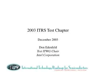
Node130 90 65 45 32 22 nm 2000 01 02 03 04 05 06 07 08 09 10 11 12 13 14 15 2016 KrF(248nm) ArF(193nm) F2(157nm) NGL Extreme Ultraviolet [EUV(13nm)] Electron Projection Lithography (EPL) Maskless Lithogaphy (ML2) Ion Projection Lithography (IPL) Proximity Electron Lithography (PEL) Proximity X-ray Lithography (PXL) Lithography Potential Solutions2001/2002 ITRS [“Unchanged” as of Tokyo Meeting, Dec’02] Source: Fukushima-san “White Paper” and Presentation
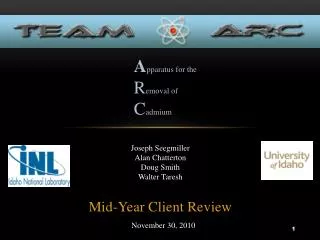
3-year Node-Cycle 2-year Node-Cycle 3-year Node-Cycle 03 04 2020 Source: STRJ, ITRS PIDS ITWG Survey, ca. 2Q03 ITRS 2003: 2003/100(-110nm?) - 2019/16nm: Average 0.5x/2.5years
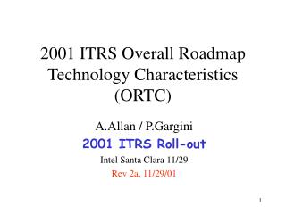
Masuhara (IRC 4/2): One Possible [Logic Half-Pitch] Solution: Stay Technology Node Unchanged but To Define and Describe the Logic Half Pitch (=Pitch/2) as M1 in the 2003 ITRS • (3) UncontactedPoly Pitch • Metal pitch • =Cell Pitch • (2) Contacted • Metal 1 (M1) pitch Logic MPU/ASIC DRAM
Wire Via • (2) Contacted • Metal 1 (M1) pitch Logic Logic Interconnect M1 Pitch [Half-Pitch (HP) = Pitch/2] (M1 Pitch) Reevaluation of transistor design, complexity is increasing.
ORTC 2003 Node and Technology Target Timing • “Final Approach” 7/15/03 • Per 7/15 IRC Meetings: • April: ITWGs were asked to prepare a “most aggressive” • “Working Approach”: • 90nm/2003 PULL-IN DRAM HP Node Header • Trade-off with delayed 6f2 Design Factor from 2003 to 2001 • 2) July IRC Meetings: Return Nodes to 2001/2002 ITRS – • “Working Approach” could not be validated by 2 Manufacturers • ITWGs re-work tables • 3) Added official ITRS DRAM hpXX Node indicator to differentiate • from Logic “Node”* “Press Releases.” • 4)UNCHANGED: MPU/ASIC Half-Pitch ORTC “Targets” • - Presently based on Metal OR Poly Pitch - Make consistent • with 2001 ITRS Interconnect TWG “Local Interconnect” by: • - Added: METAL 1 (M1) Pitch/2: 120nm/2003 (then 3yr cycle) • 5) UNCHANGED ORTC Gate-Length “Targets” • - Except re-label ASIC Operating Low Power Line Item • * Not official ITRS line item yet - include in ORTC Text for : • New M1 Half-Pitch numbers plus Logic “Node” calculation [(M1 prHP + prGL)/2]
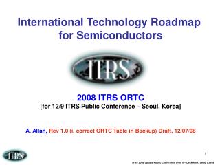
2001/2002 ITRS [“Unchanged” as of Tokyo Meeting, Dec’02] Lithography Exposure Tool Potential Solutions 2001 ITRS First Year of IC Production 1999 2001 2004 2007 2010 2013 248nm 180 248nm + PSM 130 193nm 193nm + PSM 157nm Narrow 90 EPL Options XRL DRAM Half Pitch IPL (Dense Lines) 157nm + PSM Technology Options at Technology Nodes (DRAM Half Pitch, nm) EPL Narrow EUV 65 Options IPL XRL EBDW EUV Narrow EPL 45 Options IPL EBDW EUV EPL Narrow 33 IPL Options EBDW INNOVATIVE TECHNOLOGY Research Required Development Underway Qualification/Pre - Production This legend indicates the time during which research, developmen t, and qualification/pre - production should be taking place for the technology solution. Note: Production level exposure tools should be available one y ear before first IC shipment.
Jan 2003 IRC 2003 ITRS Renewal ORTC Table Header/”Targets”: 2003 ITRS Technology Node Header (**90nm/2003 Unchanged from 2001/2002 ITRS):Near-Term Long Term Notes ---------------------------------- --------------- ----- 2003 2004 2005 2006 2007 2008 2009 2010 2013 2016 2019 hp90 hp65 hp45 hp32 hp22 hp16 DRAM Unchanged IS 100 90 80 70 65 57 50 45 32 22 16 Other ORTC Tracked Technology Trends (optional - use by TWG Tables as needed): NEW M1 Addition: 120 107 95 85 75 67 60 54 42 30 21 UNCHANGED: MPU Pr GL WAS/IS: 65 53 45 40 35 32* 28* 18* 20* 14* 10* MPU Ph GL WAS/IS: 45 37 32 28 25 22* 20* 32* 14* 10* 7* Logic “Node” ****:93 80 70 63 55 50 44 22* 31 22 16 * Not visible in 2001 ITRS due to no "annualized" columns between "Near Term" and "Long Term" column ranges. ** 90nm DRAM Half-Pitch unchanged, but cell design factor has changed, increasing cell size. Node timing based on original 2001 ITRS glossary definition of 10Ku/mo manufacturing on Production-Capable Equipment and Mat’ls. *** UNCHANGED (Poly), but need to add “Metal 1” (M1) and correlate with IC TWG “Local Wiring”/2: 120nm/’03, then 3-year target cycle (parallelto DRAM HP); ****Logic “Node” ~= [(printed half-pitch (M1) + Printed Gate Length prGL)/2], but is not included in ORTC table - only discussed in text, and with press to explain public announcements which differ in half pitch from DRAM Node. ** ***
ORTC Technology Node and Technology Target Table 1a – Near Term [Unchanged from 2001/2002]
ORTC Technology Node and Technology Target Table 1b – Long Term [Unchanged from 2001/2002]
2002-2003 ITRS No Changes from 2001 ITRS [Except Add Metal 1 (M1)] 1000 M1 Half Pitch [Actual, also same as 2001 ITRS Interconnect TWG “Local Interconnect”] 2001 MPU Printed Gate Length 2001 MPU Physical Gate Length Technology Node - DRAM Half-Pitch (nm) 100 2001 DRAM ½ Pitch 2001 MPU/ASIC ½ Pitch (Poly) Logic M1 HP 2-year “2001 ITRS DRAM HP/ Node” Cycle 3-year Cycle 10 Logic prGL 1995 1998 2001 2004 2007 2010 2013 2016 Year of Production Source: 2001 ITRS - Exec. Summary, ORTC
Lithography Exposure Tool Potential Solutions 2001 ITRS First Year of IC Production 1999 2001 2004 2007 2010 2013 248nm 180 248nm + PSM 130 193nm 193nm + PSM 157nm Narrow 90 EPL Options XRL DRAM Half Pitch IPL (Dense Lines) 157nm + PSM Technology Options at Technology Nodes (DRAM Half Pitch, nm) EPL Narrow EUV 65 Options IPL XRL EBDW Litho TWG “Production” EUV Narrow EPL 45 Options IPL EBDW EUV EPL Narrow 33 IPL Options EBDW INNOVATIVE TECHNOLOGY Research Required Development Underway Qualification/Pre - Production This legend indicates the time during which research, developmen t, and qualification/pre - production should be taking place for the technology solution. Note: Production level exposure tools should be available one y ear before first IC shipment. STRJ “Actual” “Customer Qual/Volume Ramp” 130nm/8f2/2002 F ’cast: 90nm 2004 Litho TWG “Qualification/ Pre-Production”
Node* hp130** hp90 hp65 hp45 hp32 hp22 nm 2000 01 02 03 04 05 06 07 08 09 10 11 12 13 14 15 2016 45nm 22nm 32nm Develop Develop Develop Ramp Ramp Alpha Alpha Alpha Beta Beta Beta Prod Prod Prod Qual/Pre-Prod Qual/Pre-Prod KrF(248nm) Ramp Qual/Pre-Prod ArF(193nm) F2(157nm) NGL Extreme Ultraviolet [EUV(13nm)] Electron Projection Lithography (EPL) Maskless Lithogaphy (ML2) Ion Projection Lithography (IPL) Proximity Electron Lithography (PEL) Proximity X-ray Lithography (PXL) Lithography Potential Solutions2001/2002/2003 ITRS “Unchanged”* [except 6f2 DRAM cell area factor delayed until 2008 (WAS 100nm6f2 in 2003] hp16 18 2019 ** STRJ Actual: 130nm DRAM Production 2002 ** 2003 ITRS Monitor: 100-110nm DRAM Production 2003
2003 ITRS ORTC Update Summary • 2001/2002 DRAM Technology Node UNCHANGED again for 2003 • 90nm expected early in 2004 • Aggressive proposal for 100nm/6f2 vs. 90nm/8f2 DRAM cell area tradeoff in 2003 could not be verified for 2 companies • 130nm Technology, introduced in 2001, ramped in production “early in 2002” • 100-110nm Production Announcements will be monitored in 2003 • 90nm Production Announcements in 2004 will be monitored during the 2004 ITRS Update • Previously-anticipated Transition to 3-year Nodes appears to be underway, as process complexity and implementation timing increase but we did not miss by much • Lithography is not a limiter to 65nm Node, maybe 45nm Node • Timing of future Beta and Production tools and Materials by Suppliers will be crucial to preserve the 3-year Node Cycle – must occur 2-3 years in advance of node production targets • ROI still a challenge due to long lead times to full industry volume ramp • (Based on 20K-200K wafer-starts-per-month) from first Alpha tool demo) • Semiconductor Customer final product qualification can range 1-12 months • Lesser Bits-Per-Chip (to enable ~flat chip size goal) Model needed to reflect latest actual industry practice (PIDS Survey) • Logic Contacted Metal 1 (M1) half-pitch validated and correlated to 2001 Interconnect TWG targets • Logic “Node” announcements have been correlated with ITRS Logic Half-Pitch and Printed Gate-Length • average of targets to meet both density and speed goals) • 12 announcements for 2003 Production Ramp
First Two Companies Reaching Production Original 2001 ITRS (Unchanged in 2002 Update) Production Ramp-up Model and Technology Node “Figure 2” 100M 200K Development Production 10M 20K 1M 2K Volume (Parts/Month) Alpha Tool Beta Tool Production Tool 100K Volume (Wafers/Month) 200 10K 20 First Conf. Papers 1K 2 0 12 24 -24 -12 Months Source: 2001 ITRS - Exec. Summary Figure 2 3
(Cell Array Area / Chip Size) x 100 = Cell Array Efficiency (%): Chip Size = (A x f 2 x Nbits)/CAE Cell Array Area = Cell Area x number of bits (2 n) f 2 Cell Area = Cell Area Factor (A) x f 2 ; f = technology node (half-pitch) feature size; Example: Cell Area = 2x4 x f 2 = 8 f 2 Chip Size Model Calculation Illustration - DRAM