Download
1 / 2
20 likes | 158 Views
GOALI: Epitaxial Growth of Perovskite Films and Heterostructures by Atomic Layer Deposition and Molecular Beam Epitaxy John G. Ekerdt, University of Texas at Austin, DMR 1006725.

E N D
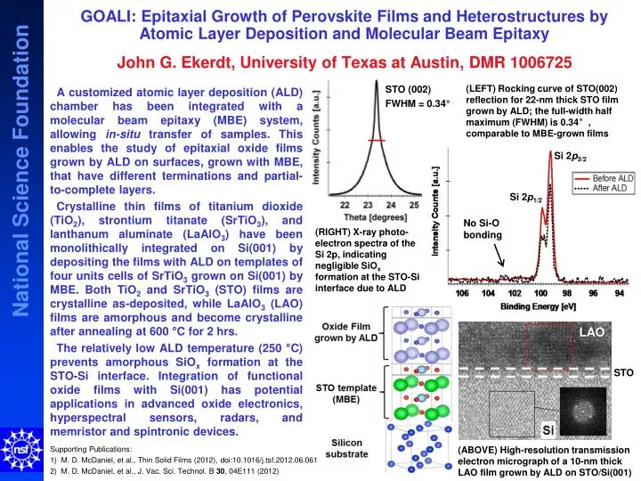
GOALI: Epitaxial Growth of Perovskite Films and Heterostructures by Atomic Layer Deposition and Molecular Beam EpitaxyJohn G. Ekerdt, University of Texas at Austin, DMR 1006725 A customized atomic layer deposition (ALD) chamber has been integrated with a molecular beam epitaxy (MBE) system, allowing in-situ transfer of samples. This enables the study of epitaxial oxide films grown by ALD on surfaces, grown with MBE, that have different terminations and partial-to-complete layers. Crystalline thin films of titanium dioxide (TiO2), strontium titanate (SrTiO3), and lanthanum aluminate (LaAlO3) have been monolithically integrated on Si(001) by depositing the films with ALD on templates of four units cells of SrTiO3 grown on Si(001) by MBE. Both TiO2and SrTiO3 (STO) films are crystalline as-deposited, while LaAlO3 (LAO) films are amorphous and become crystalline after annealing at 600 °C for 2 hrs. The relatively low ALD temperature (250 °C) prevents amorphous SiOx formation at the STO-Si interface. Integration of functional oxide films with Si(001) has potential applications in advanced oxide electronics, hyperspectral sensors, radars, and memristor and spintronic devices. Supporting Publications: 1) M. D. McDaniel, et al., Thin Solid Films (2012), doi:10.1016/j.tsf.2012.06.061 2) M. D. McDaniel, et al., J. Vac. Sci. Technol. B 30, 04E111 (2012) (LEFT) Rocking curve of STO(002) reflection for 22-nm thick STO film grown by ALD; the full-width half maximum (FWHM) is 0.34°, comparable to MBE-grown films STO (002) FWHM = 0.34° (RIGHT) X-ray photo-electron spectra of the Si 2p, indicating negligible SiOx formation at the STO-Si interface due to ALD Si 2p3/2 Si 2p1/2 LAO No Si-O bonding STO (ABOVE) High-resolution transmission electron micrograph of a 10-nm thick LAO film grown by ALD on STO/Si(001)
GOALI: Epitaxial Growth of Perovskite Films and Heterostructures by Atomic Layer Deposition and Molecular Beam EpitaxyJohn G. Ekerdt, University of Texas at Austin, DMR 1006725 We have continued the Demkov-initiated outreach Program Alice in Wonderland (AIW), initially funded under the NSF grant DMR-0606464. The program is aimed at attracting high-school female students to physical sciences and engineering; in collaboration with the physics instructors in local high schools, the students spend summers in research groups at the University of Texas at Austin and participate in “real science” in a supportive environment. The program has two parts, the summer camp and labs. After the summer camp is finished, the AIW participants work in their chosen research groups for a month or longer. Students learn from the hands on experience about advanced subjects such as a single spin detection, optical properties of nanoparticles, magnetic atomic force microscopy (AFM), atomic layer deposition (ALD) growth of thin films, biophysics, and first principles calculations. They interact with a large group of faculty, graduate and undergraduate students. (Top) AIW participant presenting a lecture on “Experimenting with Micro-spheres”; (bottom) the 2012 AIW students in the Materials Physics Lab