Download

1 / 12
160 likes | 686 Views
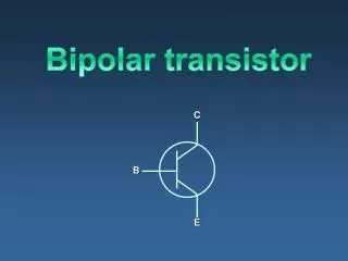
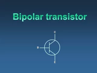
מכללה האקדמית אורט בראודה המחלקה להנדסת חשמל ואלקטרוניקה מוליכים למחצה 31350. תרגול מס' 14. Bipolar Transistor. (BJT - bipolar junction transistor). Bipolar Transistor. Bipolar transistor was invented by Walter Brattain, John Bardeen and William Shockley (Bell Labs) in 1949.

E N D
מכללה האקדמית אורט בראודההמחלקה להנדסת חשמל ואלקטרוניקה מוליכים למחצה 31350 תרגול מס'14. Bipolar Transistor (BJT - bipolar junction transistor)
Bipolar Transistor Bipolar transistor was invented by Walter Brattain, John Bardeen and William Shockley (Bell Labs) in 1949. It is a 3-terminal device, which is usually used as an amplifier or a switch. Examples of typical bipolar transistors 3D sketch of pnp bipolar transistor
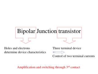
What is Bipolar Transistor ? Bipolar transistor is a semiconductor device with two interacting PN-junctions, connected together in series back-to-back. two types of bipolar transistors: the Base HAVE TO be short enough to allow crosstalk between the Emitter and the Collector arrow symbol ↔ Emitter arrow direction ↔ current direction Outstanding guide on npn transistor
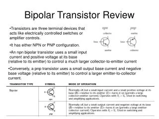
Bipolar Transistor modes cutoff saturation In cutoff, biasing conditions are opposite to those of saturation, namely, both junctions are reverse biased. There is very little current flow, which corresponds to a logical "off", or an open switch. With both junctions forward-biased, a BJT is in the saturation mode and facilitates high current conduction from the emitter to the collector. This mode corresponds to a logical "on", or a closed switch. active reverse-active By reversing the biasing conditions of the forward-active region, a bipolar transistor goes into reverse-active mode. In this mode, the emitter and collector regions switch roles. The βF in inverted mode is several times (2–3 times for the ordinary Ge BJT) smaller than that of active mode. (Seldomly used mode.) In the active mode, the emitter–base junction is forward biased and the base–collector junction is reverse biased. Most of BJTs are designed to afford the greatest common-emitter current gain, βF, in the active mode. If this is the case, the collector–emitter current is approximately proportional to the base current, but many times larger, for small base current variations.
Band diagram of BJT (active mode biased pnp) EF quasi electrons holes holes Emitter Collector Base
Basic idea of BJT Emitter - Base junction is asymmetric: Thus, the Emitter’ hole current is controlled by Emitter - Base junction The width of the neutral region of the Base is small (much less than the holes diffusion length): Therefore most holes diffusing into the Base will reach the Collector
Current flow (active mode - pnp) magnetta – current of holes rose – current of electrons • Emitter – Base currents (EB junction is forward-biased) • holes diffusing from the Emitter to the Base • electrons diffusing from the Base to the Emitter • Base currents • (3) recombination of holes injected into the Base • (4) most holes reach Collector since • Base – Collector currents (BC junction is under reverse bias) • (5) electron (minority carrier) current from Collector to Base • (6) hole (minority carrier) current from Base to Collector can be neglected for most practical purposes
BJT principle of operation (active mode - pnp) magnetta – current of holes rose – current of electrons בטרנזיסטור pnp, חורים (מטעני רוב ב- emitter) הוזרקים דרך צומת PN emitter-base (הנמצא בממתח הקדמי) לאזור ה- base. חלק מהחורים עושים רקומבינציה עם אלקטרונים (מטעני רוב ב- base), חלק אחר חוזרים בחזרה (ע"י סחיפה) ל- emitter. אבל היות וה- base הוא דק מאד ומסומם יחסית מעט, רוב החורים, שהוזרקו מה- emitter, מצליחים להגיע (ע"י דיפוזיה) עד לאזור המחסור בצומת collector-base. צומת PN זה (base – collector) נמצא בממתח האחורי. השדה החזק של הצומת לוקח את החורים (להזכיר, כי חורים הם מטעני מיעוט ב- base ובשבילם הצומת הוא פתוח) ומעביר אותם ל- collector. לכן זרם ה- collector כמעט שווה לזרם ה- emitter (מלבד החלק הקטן שנאבד ב- base עקב רקומבינציה) : . המקדם המקשר בין זרם ה- emitter לזרם ה- collector (המקדם ) נקרא מקדם המעבר של זרם ה- emitter. בדרך כלל משתנה בין 0.9 ל-0.999 . ככל ש- גדול יותר, כך העברת הזרם ע"י טרנזיסטור היא יעילה יותר. יש לציין, כי כמעט ולא תלוי במתחים ו- . בהמשך נראה, כי המקדם המקשר בין זרם ה- base לזרם ה- collector (המקדם ) מתבטא דרך המקדם בצורה הבאה: . מעצם העובדה ש- כמעט ולא תלוי במתחים בצמתים, נובע, כי גם בטווח רחב של מתחים נשאר קבוע. לכן, ע"י השינוי בזרם החלש של base, , ניתן לשלוט בזרם החזק של ה- collector , . Thus the (small) base current controls the (strong) collector current
Basic amplifier circuits common-base configuration input output = current amplification in common-base circuit Since , typical values for are: By setting and we control and
Basic amplifier circuits common-emitter configuration output input = current amplification in common-emitter circuit The gain, , is determined by doping is very sensitive to : By setting and , we control and
Basic amplifier circuits common-collector configuration (grounded collector or Voltage Follower or Emitter Follower) input output = current amplification in common-emitter circuit By setting and , we control and
References • B. Streetman, S. Banerjee, “Solid state electronic devices” (6th edition), Prentice Hall, 2005. • B. Streetman, S. Banerjee, “Instructor’s solutions manual to the “Solid state electronic devices” ” (6th edition), Prentice Hall, 2005. • B. Van Zeghbroeck, “Principles of semiconductor devices”, Lectures – Colorado University, 2004. • D. Neamen, “Semiconductor Physics and Devices: Basic Principles” (3rd edition), McGraw Hill, 2003. • D. Neamen, “Semiconductor Physics and Devices: Basic Principles” (3rd edition) – Solutions manual, McGraw Hill, 2003.