Download
1 / 21
210 likes | 359 Views
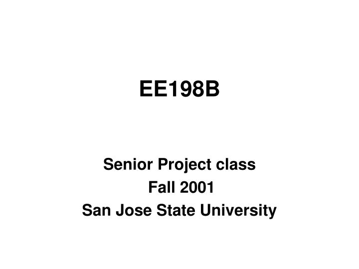
EE198B. Senior Project class Fall 2001 San Jose State University. Single Crystal Solar Photocell. Team Members: Mack Appleton Sung Min Park Yemane Tsegaye Angel Milano Project Advisor: Dr. David Parent . Project Outline. Introduction Initial Testing Design and Simulation.

E N D
EE198B Senior Project class Fall 2001 San Jose State University
Single Crystal Solar Photocell Team Members: Mack Appleton Sung Min Park Yemane Tsegaye Angel Milano Project Advisor: Dr. David Parent
Project Outline • Introduction • Initial Testing • Design and Simulation. • Fabrication of Solar Cells • Test Solar Cells • Conclusion
Project Objective • To design, simulate, establish and document a silicon process base-line traveler for the Single Crystal Solar Photocell. • To enhance the relative efficiency of the Solar Photocells by 5%.
Design and Simulation Maximize the efficiency Anti-refraction coating.
Formula & Equations 1. Rs=L/w (2D) 2. Rs = (Rn+) + (Rbar) + (Rcontact) Rn+ = (n+ * S)/(n*b) Rbar = (al*b)/(Wb*n) Rcontact = c/(Wb*b) 3. = Pm/Pin = (FF*IL*Voc)/Pin 4. FF : Fill Factor (Im*Vm)/(Isc*Voc) 5. P=I*V= (I^2)*R
Design of Models Large-grid with AR Large-grid without AR Small-grid with AR Small-grid without AR where Large grid : S=3.3 cm, Wb=0.2cm, b=6.6cm, and 2 fingers. Small grid : S=0.75cm, Wb=0.2cm, b=6cm, and 8 fingers
Fabrication of Solar Cells • Diffuse donor region • Apply aluminum coating to front of wafer • Photolithography to define solar cell pattern • Etch aluminum to create solar cell pattern • Apply anti-reflection coating * • Apply aluminum coating to back of wafer • Anneal wafers • Remove outer edges of wafers
Diffuse Donor Region • Spin on phosphorous doped silica glass • Apply 3ml to front of wafer • Spin @ 3000 rpm for 20 seconds • Diffuse in furnace • Heat furnace to 1100oc • Push in wafers ½ inch per 15 seconds • Diffuse for 1 hour • Pull out wafers ½ inch per 15 seconds • Makes wafer into a large diode
Apply Aluminum Coating • Desire 2 microns thickness • Sputter on the aluminum • Accurate and precise • Fast (2 microns onto 8 wafers in 15 min.) • Prone to breaking down - Or - • Evaporate on aluminum • Reliable • Slow (2 microns onto 24 wafers in 3 to 4 hours) • Not very precise
Photolithography • Apply 3ml photo-resist; Spin for 20s @ 5000 rpm • Soft bake for 90oc for 30 minutes • Place solar cell mask on wafer • Place both into wooden and glass holder • Expose under lamp for 2 minutes • Develop for 15 seconds
Etch Aluminum • Etch exposed al using hot sulfuric acid • Rinse with DI water • Remove remaining PR using plasma etch
Apply Anti-reflection Coating • Apply 3ml Titaniumsilicafilm • Spin @ 3000 rpm for 20 seconds • Spreads film to thickness of 1000 angstroms
Anneal Wafers • Anneal for 30 minutes in furnace • Creates ohmic contact between al and Si
Cleave Edges of Wafers • Need to prevent shorting along edge of wafer • Use scribe tool to score along edges of solar cell • Cleave wafer along scoring
Testing the Solar Cells • Scored, or roughened, back of cells • Placed onto roughened aluminum wafer • Used probes to make contacts • One probe onto the corner of the cell’s al grid • One probe onto the al wafer • Tried various methods for making good contacts • Solder paste • Silver paste • Copper tape
Testing the Solar Cells • Illuminated the cell • Used 75W light bulb at 3cm distance • Connected voltmeter to probe terminals • Gives open circuit voltage • Connected current source to probe terminals • Ran current against that being generated by the cells • Measured voltage for different current levels
IV Curves for One Half ofGrid Solar CellsPmax S13A = 41.9 mW Pmax S6A = 49.8
IV Curves for Small Grid Solar CellsPmax S21 = 61.4 mW Pmax S8 = 71.5 mW
Conclusions • AR cells average of 17.8% more efficient • Efficiency increase = (PmaxOLD – PmaxAR)/PmaxOLD • Wanted minimum 5% increase • Easy to follow process • Recommendations • Use the smaller grid • Possible photolithography and etch of back al