Download
1 / 27
290 likes | 533 Views
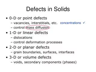
3.3.3 Defects in the silicon film. 3.3.3.1 Most common defect The most common defects in SOI layer COPs, dislocation, HF defects (1)COPs (crystal-originated particle or crystal-originated pit) ・すべての Si wafer(bulk, SOI wafer を含む ) の基板の欠陥 ・八面体の空間

E N D
3.3.3 Defects in the silicon film 3.3.3.1 Most common defect The most common defects in SOI layer COPs, dislocation, HF defects (1)COPs (crystal-originated particle or crystal-originated pit) ・すべてのSiwafer(bulk, SOI waferを含む)の基板の欠陥 ・八面体の空間 ・SOI薄膜中、COPsはtopとbottomのSi膜を交わる ⇒bottomからtopのSi膜をつなぎあわせる“pipe”が形成 COPsはepitaxial layer上では起こらない SOI-seminar-0921
(2)Dislocations SOI物質中で見つかる主な欠陥 <SIMOXの場合> Si/buried oxide interfaceからSiのoverlayerの表面に垂直にあるズレをつなぎあわせる dislocationの存在はyieldなどの問題を引き起こす可能性がある 金属の不純物:diffuse to dislocations upon annealing dislocation :gate oxideのweak pointを生じさせる low breakdown voltageが観測 <Early study> SIMOX上のgate oxideの成長のintegrityはSi bulk上のoxide成長のintegrityに匹敵 SOI technology: dislocation density や金属不純物の準位の改良が必要 SOI-seminar-0921
(3) HF defects Si薄膜中のsilicides, silicatesの金属混合物からなる 純粋なSiとは違い、HF(フッ化水素)と反応 waferがHFに浸されると、小さな穴がSi薄膜中で形成 etchtimeが十分に長い ⇒SOI filmの底のBOXもetchされる SOI-seminar-0921
TEM: ・crystal defectの分析において有効な techniqueの1つ ・限られた大きさのサンプルで分析可能 <TEM cross-section> サンプルの直径:幅20μm 深さ0.7μm ⇒maximum observable area: 10-7cm-2 minimum measurable defect density :107defects/cm2 平面方向:より大きなサンプル領域で測定可 sample holderの大きさの領域で分析可 (7mm2grid) に限られる SOI-seminar-0921
倍率が10,000を下回るとdislocationの測定が困難 この場合 測定領域:10-5cm2 minimum observable defect density: 105 defects/cm2 <TEM測定> lengthy, delicate sampleが必要 <Defect decoration technique> optical microscopyと組み合わせて利用 ☆サンプルの特性やdefectsの条件を満たすとき、 TEMのほうがよく使われる SOI-seminar-0921
3.3.3.2 Chemical decoration of defects • SOI defects decoration で使われるetchmixtures (Table3-2) 酸化剤 (CrO3, K2Cr2O7,,HNO3) とHFの混合物からなっている SOI-seminar-0921
<Defect decoration> Siに関してはhigher etch rateによる欠陥 <Decoration> high-disorder defect(層と層の境界)に最も効果的 etch rate of Si :1μm/min (Dash ,Secco , Stirl, Wright etch solution) Schimmel etch rate:これらよりかなり低い SOI薄膜のdecoration of dislocationはclassical etch mixtureを使うのは不可能。 <理由> すべてのSiは効率的なdecoration of defectができる前に取り除かれてしまうため Lower etch rate:etch溶液を水で希釈することにより実現可 SOI-seminar-0921
< electrochemical etching > ・もう1つのdecoration technique ・5%に希釈されたHFはSOI薄膜中での結晶欠陥を明らかにする ・n-type(Nd≒1015cm-3)doseのSiのoverlayerが必要 ohmic接触はサンプルのfront side、back sideで起こる <方法> 5%のHF中で10~30分間行われる 3つの電極を使う ①、②Siを3Vでコントロールするもの(±) ③Ca/CuF2 reference電極 decoration techniqueは defect-free Siではetchされない SOI-seminar-0921
・dislocation of defect ・metal contamination-related defect ・oxidation-induced stacking faults Si薄膜中に穴を開ける optical microscopy:観察とdecoration後の穴の数を 数えるのに使われる <etch rate> Secco etch⇒SOI薄膜に使う場合、高すぎる optical microscopyでの観察した際、欠陥が明らかになる前にすべてのSi薄膜がetchされてしまう。 Secco solutionの希釈でetch rateを減らしている SOI-seminar-0921
SeccoとHF etchのcombination ⇒SOI薄膜の欠陥を発見しやすくしている Seccoの希釈 ⇒Si layer中でのdecorate defectを見つけるのに初めて使われた Secco etchによって穴が開けられる段階では 顕微鏡の観察では十分な対比が得られない ⇒サンプルはHF中に浸される ⇒酸はSi膜中の穴を貫通させ、buried oxideをetchする ⇒oxide上でetchされ、円形の模様はSi layerを貫通して見える より精巧な方法 “transferred layer etch” SOI-seminar-0921
3.3.3.3 Defection of defects by light scattering 欠陥:wafer表面でのlaser光の散乱を使うことで検出可 <Defect-mapping system> 製造工程でのwaferをモニタするのに使われる scattering centerを検出するように設計されている Si film中での欠陥、粒子による欠陥 これらのcenterではbackground scattering noise に対して区別されている <測定system> bare Si waferに換算 waferの”haze”と呼ばれている SOI-seminar-0921
SOI waferはSiと異なる反射率を持つ <SOI waferの反射率> ・BOXやSi filmの厚さに比例 ・Siの反射率よりも高くしたり、低くしたりできる “shiny”“dark” SOI waferの反射率 SOI-seminar-0921
bare Si waferとの補正を使うと、 laser scattering defect systemは ①shiny waferの欠陥は大きく、 dark waferの欠陥は小さく見積もってしまう ②background hazeの準位はwaferの反射率に反比例 これらの問題を避けるためにUV laserの使用が提案 • Si中のUV lightのabsorption depthはとても小さい • 内部反射や反射率のfilmの厚さの依存性はUV laserの使用によって推測可能 SOI-seminar-0921
3.3.3.4 Other defect assessment techniques • Impulsive Stimulated Thermal Scattering (ISTS) ⇒SOI waferのdefect densityを評価するのに使用 <特徴> ・contactless ・non-destructive ・opto-acoustic(光エネルギー音波に変換) 交差した励起ビームの対からのlaser光のパルス (λ=532nm) laserのエネルギーの吸収は サンプル中で熱膨張する SOI layerの表面で 干渉縞を作る SOI-seminar-0921
順々に急な熱膨張によって生じるacoustic wave を作り出す 同時に、 サンプルは強さの低いlight beamやサンプルから反射される 回折した信号によって分析される SOI wafer上で、 最初の熱励起後の回折された信号が指数的に減衰するとき、 信号のピークの大きさはdefect densityに対応 この手法は Secco etch pit microscopic observationに対して補正され、 10%以内の再現性を持つ 時間依存性を持ち、 acoustic wave physicsのモデルによって分析される SOI-seminar-0921
<Photoluminescence (PL)> 電子の光励起 波長の観測 励起後の光子再放射の強さ に基づく <PL測定> ・液体He(4.2K)と室温(300K)の間の温度で行われる ・電子はlaser beamによって価電子帯から伝導帯へ飛び上がる ・プローブできる深さ領域⇒laserの波長に依存 5~10nmから1~3μm UV laser 可視光 SOI-seminar-0921
生成後、 ・バンドの端と端で電子は再結合 ・電子は1つまたはいくつかの深さの準位を通過 電子がradiative recombination centersとしてふるまう ⇒欠陥は直接的に明らかになる 光励起によるcarrierのほとんど ⇒欠陥準位を経て、non-radiativelyに再結合 non-radiative process ⇒効果的な再結合のlifetimeを決定 バンドとバンドの再結合でのphotoluminescenceの信号の大きさはlifetimeに比例 ⇒信号の大きさの変化は欠陥分布に影響をもたらす SOI-seminar-0921
<deep-level photoemission signal> 生成のlifetimeやdeep-level defect濃度に比例 ⇒deep-levelでの放出の大きさの変化は固有の欠陥分布の情報を与える <PL system> SOI waferのmap defectに使用 <dislocation, stacking faults, metal precipitates> 欠陥のまわりでlifetimeの減損が局在化されるところで観測される SOI-seminar-0921
3.3.3.5 Stress in the silicon film <Raman microprobe technique> Si film中でSOI fabrication process, device processによって生じるstressを測定 Ar laser(λ=457.9nm)のビームをサンプルに照射 測定領域:0.6μm 小さい! 反射されたビームのスペクトル virgin bulk Siによって与えられるスペクトル スペクトルのピークのシフト 半値幅(FWHM) 比較 Si film上のstressの大きさの情報を与える SOI-seminar-0921
3.3.4 Defect in the buried oxide <buried oxide> “pipes”と呼ばれる欠陥を含むSIMOXからできている <Si filament> buried oxideを通ってSOI layerからsubstrate につながっている pipe map分布はFig3-9のように作られ、直径も推定される SOI-seminar-0921
CuSO4に浸され、SOI waferと銅電極にはさまれる waferの端のSi filmはTexwipeと接触 waferのbackはAl電極と接触 電圧がかかっていると、電流はpipesに沿ってBOXを通過して流れる <電解反応> CuSO4→Cu2++SO42- Cu2++2e-→Cu (s) 銅のstainはTexwipeで作られる 1つのpipeから電流を受けて、Texwipe内で起こる SOI-seminar-0921
<stainの直径> 各pipeに流れる電流に比例 ⇒pipeの幅が広いほど、stainの大きさは大きい pipeが円筒だと考えたときの直径dは次のように表せる ohm’s lawより d pipe (3.4.1) I:pipeを流れる電流 ρ:Siの抵抗率 tBOX: BOXの厚さ V : 印加電圧 SOI-seminar-0921
<calculation> 2つの電子から、 1つの観測可能な銅stainを作り出すときの pipeの直径の最小値が5nmだと推測できる SOI waferを通る電流によっても同様な結果が得られる copper stainが直接waferに沈殿している場合、 SOI wafer自身でpipeの直径を推測できる copper nitriteとメタノールを混ぜた溶液に浸されている SOI-seminar-0921
3.3.5 Bond quality and bonding energy ☆wafer間のbondのqualityやstrengthの評価は重要。 Wafer bonding:BESOI, Smart-Cut, Eltran のpreparation に使われる技術 infrared transmission imaging:bouned wafer間のvoidの存在 を探すのに使用 <IR-imagingのset-up> 白熱灯と赤外線カメラを使用 SOI-seminar-0921
bond strength:[erg/cm2] or [J/m2]の単位で測定 *1 erg/cm2 = 10-3 J/m2 bond energyの測定:(1)crack propagation technique bond energyγ tb:bladeの厚さ L : crackの長さ[m] tw :各waferの厚さ[m] E :silicon Young’s modulus[166GPa] 長所:行うのが簡単 短所:Lに揺らぎがあるときγが不確かになる 例)Lが10%の不確かさ⇒γは50%のerror SOI-seminar-0921
<Young modulus> :硬さを表す値 断面積S,長さLの弾性体を力Fで引っ張ったときに 長さδLだけ伸びたとする。 このとき、 <応力> σ=F/S <歪> ε=δL/L <Young率> E=σ/ε 単位 [Pa] or [N/m2] L δL F S SOI-seminar-0921
bond energy測定:(2)classical Vickers indentation Technique Vickers indenter: diamond-tipped, square-based pyramidal hardness of metal,壊れやすい物質(ceramics, glass)の測定に使用 bond interfaceに沿った crackの長さ ⇒bond energyの測定 Kic∝ toughness of the material P: Vickerstoolに与える力 2c:crackの長さ β: geometrical factor ν: Poisson ratio, E:Young’s modulus SOI-seminar-0921