Download
1 / 2
20 likes | 185 Views
Flexible, Low Voltage and Low Hysteresis Ambipolar and Unipolar PbSe Nanowire Field-Effect Transistors Cherie Kagan , University of Pennsylvania, DMR 0805155.

E N D
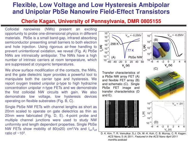
Flexible, Low Voltage and Low Hysteresis Ambipolar and UnipolarPbSeNanowire Field-Effect TransistorsCherie Kagan, University of Pennsylvania, DMR 0805155 Colloidal nanowires (NWs) present an exciting opportunity to probe one-dimensional physics in different materials. PbSe is a small band-gap, infrared absorbing semiconductor presenting small barriers to both electron and hole injection. Using rigorous air-free handling to prevent unintentional oxidation, we reveal (Fig. A) PbSe NWs are intrinsically ambipolar. The NWs have a high number of intrinsic carriers at room temperature, which are suppressed at cryogenic temperatures. We show surface modification of the contacts, the NWs, and the gate dielectric layer provides a powerful tool to manipulate both the carrier type and hysteresis. We report oxygen treated unipolar p-type to high hydrazine concentration unipolar n-type FETs and we demonstrate the first colloidal NW circuits with gain. We also demonstrate low voltage, low hysteresis devices operating on flexible substrates (Fig. B, C). Single PbSe NW FETs with channel lengths as short as 20nm scaled to operate on gate dielectrics as thin as 20nm were fabricated (Fig. D, E). 4-point probe and multiple channel junctions were used to study NW uniformity and length dependent properties. Single PbSe NW FETs show mobility of 80(±20) cm2/Vs and Ion/Ioffratio of ~103. (B) 298 K 77 K PbSe NW (A) (C) Transfer characteristics of a PbSe NW array FET (A) and flexible FET array (B) and schematic (C). Single PbSe FET image and transfer characteristics (D and E). (E) (D) • D. K. Kim, T. R. Vemulkar, S.J. Oh, W.-K. Koh, C. B. Murray, C. R. Kagan; ACS Nano, 5 (4) 2011. Featured in the ACS Nano April 2011 monthly podcast
Measuring and Demonstrating the Behavior of Nanoscale MaterialsCherie Kagan, University of Pennsylvania, DMR 0805155 Graduate students David (A) and SJ Oh (B) describes the application of nanoparticles in sunblock for Nanoday at the Franklin Institute (A) Graduate students from the Kagan group gave demonstrations on the physics of nanoscale materials to families visiting the Franklin Institute in Philadelphia for Nanoday [Fig. (A, B)]. Two undergraduate students, TarunVemulkar [Fig. (C)] and Silvia Chan [Fig. (D)], worked over the academic year with fellow graduate students to electrically probe charge transport in nanowire transistors. Controlling the nanowire environment impacts its measured transport characteristics. (B) Undergraduate students Tarun (C) and Silvia (D) who are working on the DMR project. (D) (C)