Download
1 / 38
380 likes | 477 Views
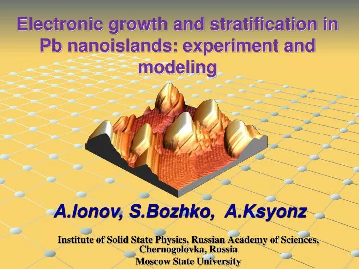
Electronic growth and stratification in Pb nanoislands : experiment and modeling. Institute of Solid State Physics, Russian Academy of Sciences, Chernogolovka , Russia Moscow State University. A.Ionov, S.Bozhko, A.Ksyonz. Outline. Pb island on Si(111). Basics of Electronic growth

E N D
Electronic growth and stratification in Pbnanoislands: experiment and modeling Institute of Solid State Physics, Russian Academy of Sciences, Chernogolovka, Russia Moscow State University A.Ionov, S.Bozhko, A.Ksyonz
Outline Pb island on Si(111) • Basics of Electronic growth • thin Pb islands on Si(111): STM experiments • Quantum size effect and models of Electronic growth • QWS in Pb/Si(111) film by ARPES and STS • Pb islands structure grown on Si(7 7 10) • Experimental • STM Results • DFT simulations • Conclusions Pb island as an abrikosov’s vortex trap Does quantum confinement effect on the crystal structure of a bulk of the Pb islands?
Status Quo Pb films on the Si(111) Pbislandsgrowth follows the Stransky-Krastanov scenario • STM images and corresponding histograms obtained after deposition 3ML of Pb at 192K (left, 200×200nm2) and at 200K (right, 300×300nm2). • Wetting layer 1-3ML depending on the deposition temperature • The islands grow up in a bi-layer growth mode - the island height changes by 2ML during the growth • Island thickness of 7ML is preferable • Islands possess a steep edges and flat tops Phys.Rev.Lett., 86, (2001) 5116-5119 W. B. Su, S. H. Chang et.al, Surface Science 493 (2001) 526-538M.Hupalo, S.Kremmer, V.Yer, L.Berbil-Bautista, E.Abram, M.C.Tringides
Quantum size effect The thickness Nt of confining well has to satisfy the requirement of energy quantization that is the electron wavefunction has to form standing waves: Pb island N,s – integers, λF-electron wave length, t-thickness of Pb(111) monolayer The island height is stable only when the requirement is met Possible stable heights for Pb(111) crystal determined by the requirement of energy quantization. The islands can be stable only when both N and s are integers (marked by red)
1-d model of electronic growth out of energy quantization requirements N=8, S=11.6 energy quantization requirements are fulfilled N=7, S=5, Nt=5λF Electron standing wave resulted in non homogeneous distribution of electron charge density. Oscillations of charge density cause open of energy gap at k=kF .
3-d model of electronic growth Confinement of the electrons to a quantum well causes the Fermi sphere of allowed states to be reduced to a discrete set of subbands. Electrons are free to move in X-Y plane -surface or electron confinementenergy – total energy of the film - total energy per atom of bulk Pb
3-d model of electronic growth N – number of Pb layers Nt – thickness of the film α =1.77±0.09 is a fitting parameter The relative surface energy is well described by the sinusoidal form φ - a phase shift factor that is dependent on the interface properties of the film 7 The essential physics of the surface energy of a metal film can be captured with a model of a free-electron gas confined to a quantum well. The surface energy for a Pb(111) film was calculated in a frame of a free-electron gas confined to a quantum well. When the Pb thickness is 7 ML, electron energy is minimal. Phys.Rev.B 72 075402 (2005) P. Czoschke, Hawoong Hong, L. Basile, and T.-C. Chiang
Growth of the Pb islands on the Si(7710) • STM 3D image of the Pb nanoislands on Si(7710)
Pb/Si(557) : LEED pattern, energy Ep=101eV. , substrate temperature 78К, 2MLPb deposited. Growth of Pb islands on Si(557): On the terrace (111) On the triple steps and terraces Pb on Si(557) Surface Science 515 (2006) 312E, Hoque, A. Petkova, M. Henzler
Experiment STM UHV 300mK « M3 » LAS-3000 equipped by RT STM GPI-300 Base pressure 10-10mbar Temperature 300K Magnetic field No Base pressure 10-11mbar Temperature 300mK Magnetic field up to 10T
Pb islands deposited on Si(7 7 10) Pb film was deposited using electron bombardment-assisted evaporation in a preparation chamber. The substrate temperature was 300K, the pressure was in the range of 2×10⁻¹⁰ Torr. STM images obtained after deposition 16 ML of Pb at room temperature.
STM image of the Pb film on Sithe drawing plane coincides with the Pb(111) island top surface b) Plot of the cross section b The red dashed line corresponds to the (7710 ) substrate. The cross-section c reveals the layered structure of the island c) Cross-section c demonstrates the top layer of the island which does not contacted the substrate surface d) Histograms of the heights in the areas 1 and 2 reveal the existence of steps 2nm in height. c)
Growth of Pb islands on Si(7710)homoepitaxial regime: Some islands cross-sections demonstrates that the top layer of 7ML in thick of the island grows without any contact with the substrate, i.e. the island grows in the homoepitaxial regime: Pb on Pb. In this case there is no any influence of the lattice mismatch on interface and elastic stresses. The reason of relaxation in this case could be the electronic growth mechanism. Possible origin for the 2nm pancake growth could lie in the electron energy term of the total energy of the island. The layer thickness statistics obtained from 12 different Pb-islands.
Pb/Si(7710)- balance of energy Conclusions -The total energy of a Pb nanoisland non-divided into layers exceeds the total energy of a lamellar island of the same size. - Defect generation is due to energy gain of both elastic stress Em and electron confinement energy ES. 7 ML The thickness of 7 monolayers Pb is the most energetically favorable, even with respect to the bulk material.
Candidates for quantum wells Twinning is a predominant mechanism of energy relaxation in face-centered cubic metals with low stacking-fault energy in (111) planes. Twin boundaries seems to be the most favorable candidate to realize the island stratification because of the low formation energy.
Twin boundaries in Pb nanoparticles Configuration transition, involving vanishing of a twin on the left side, leaving a stalking fault, and appearance of twin on the right side. (The first configuration was stable for 1.5 sec, the second configuration was stable for 6.5 sec, the transition time is less than 0.04 sec.) Phys.Rev.Lett. 78 (1997) 2585, T. Ben-David, Y. Lereah, G.Deutscher, J. M. Penisson, A. Bourret, R. Kofman, and P. Cheyssac
DFT calculations of Pb cluster The abinitiocalculationswereperformedwiththeCASTEPprogramfromMaterial Studio (AccelrysSoftwareInc.)usingResearch computing Centre of Moscow StateUniversity Crystal Pb slab within range 3-41 layers was modelling
DFT calculations of Pb cluster Perfect crystal structure Z Primitive unit B A C B A C B A C B A Calculated surface energy is fitted by Film was simulated as a Pb slab with a perfect crystal structure. Left panel represents a sequence of close-packed hexagonal planes forming FCC Pb crystal structure. The thickness of 7 monolayers Pb is the most energetically favorable The ab initio calculations were performed with the CASTEP programfrom Accelrys Software Inc. using 'Lomonosov' supercomputer of Moscow State University
DFT calculations of Pb cluster Crystal contains twinning boundary Z Primitive unit A B C A B C B A C B A The thickness of 14 monolayers that is 2 slabs with a perfect crystal structure 7 ML in thick separated by a twinning boundary possesses a negative surface energy of 9mV per atom. Bottom part of a slab is a mirror reflection of a top one System of conductive electrons generates twinning boundaries in a bulk of Pb crystal !
DFT simulation of difference in total energy per single atom located in hcp and fcc positions on the surface of slabs N monolayers in thick. Difference in atom energy in hcp and fcc position as a function of a slab thickness Atom in fcc position Atom in hcp position
Conclusions The growth of Pb-nanoislands on the vicinal Si(7710) stepped surface follows Stransky-Krastanov scenario. The growth of tilted Pb bulk islands is accompanied by theirs stratification into layers. The formation of stable blocks of equal thickness (single layer thickness 2nm, 7ML of Pb) during the growth of Pb on Si(7710) was detected – pancake structure. DFT simulations prove that the size of the blocks corresponds to energy minimum of the electrons confined in the quantum well. The layers are separated by a twinning boundaries. Such growth mode is realized due to the minimization of the electron energy owing to the quantum confinement effect and is in a good agreement with the electronic growth model.
Collaborators V.Dubost A.Ionov S.Bozhko D.Roditchev F.Debontridder T.Cren D.Fokin A.Ksyonz A.Chaika I.Sveklo
Pb/Si(7710)- balance of energy The film-substrate interface and elastic energy due to a Pb-Si lattice mismatch 2.02nm 1.89nm One Pb(111) atomic layer is 2,86Å in thick, one Si atomic step height is 3,13Å . If Pb layers are parallel to the Si(111) surface plane than the maximum lattice mismatch of 1,3Å is achieved at Pb layer thickness of 7ML. Thus, for a 2nm thick Pb slab the stress achieves its maximum. The value of elastic stress can be partially reduced by 1° tilt of Pb layers. Wetting layer also reduces elastic energy. Nevertheless the elastic stress can assist in a crystal defects generation.
Pb/Si(7710)- balance of energy Stratificated (pancake like) island Perfect crystal structure of the island – energy of interlayer defects, stress at the film – substrate interface can be reduced by interlayer defects – proportional to the number of atoms in the island – energy of layers due to quantum confinement effect , when requirements of formation of electron standing wave met in the layers – energy due to a stress at the film – substrate interface Pb Pb 2nm D D Si Si Island stratificates if energy gain due to quantum confinement effect exceeds energy loss due to creation of interlayer defect
3-d model of electronic growth N – number of Pb layers Nt – thickness of the film α =1.77±0.09 is a fitting parameter The relative surface energy is well described by the sinusoidal form φ - a phase shift factor that is dependent on the interface properties of the film 7 The essential physics of the surface energy of a metal film can be captured with a model of a free-electron gas confined to a quantum well. The surface energy for a Pb(111) film calculated using a model based on a free-electron gas confined to a quantum well. When the Pb thickness is 7 ML, electron energy is minimal. Phys.Rev.B 72 075402 (2005) P. Czoschke, Hawoong Hong, L. Basile, and T.-C. Chiang
Experiment Si(111) Si(7 7 10) flash at 1250ºC cooling to 1050ºC in 1 min quench to 850ºC LEED, Ep=60eV postanneal at 850ºC for 20 minutes slow cool down to RT STM images of the clean initially Si(7 7 10) surface showing the triple step structure with (7×7)-reconstruction on Si(111) terraces. The directions of steps edges are (-110). The height of the triple step is known to be 3,13Å×3=9,39Å
STM images of vicinal surface STM images of the clean initially Si(557) surface showing in (a): large areas covered with Si(7 7 10) stepped structure; in (b): the triple step structure with (7x7)-reconstruction on Si(111) terraces. Inset : Fast Fourier Transformation of (a) reveals two characteristic peaks corresponding to the (7 7 10) stepped structure.
Clean Si(557) surface Si(557) staircase: triple steps and terraces Si(111) (7x7). Period - 5.7nm(17 atomic rows) A.Kirakosian et al., Appl. Phys. Letters 79 (2001) 1608 Si(7710) triple steps and terraces Si(111)(7x7). Period -5.33nm (16 atomic rows) Teys et al. Surf. Sci. 600 (2006) 4878–4882 Surface consists of Si(111)7x7 terraces separated by triple steps Atomic structure of a triple steps is not clear
Triple step structureSi(557) 5,5×5,5nm2 STM image. a) Vb=-2.1V, I=80 pА, b) Vb=0,4V, I=90pА [223] [111] Triple step can be considered as a set of a single and double steps Si(223) triple steps and terraces Si(111)(7x7). Period – 4.8нм (141/3 atomic rows) A.Chaika et.al. Surf.Sci.603 (2009) 752 J.Appl.Phys. 105 (2009) 034304
FCC and HCP structures Spheres may be arranged in a single closest-packed layer by placing each sphere in a contact with 6 others. A second similar layer may be packed on top of this by placing each sphere in contact with 3 spheres of the bottom layer. In FCC the spheres in a third layer are placed over the holes in the first layer not occupied by the second layer.
Pb island superconductivity STM image of Pb film grown on Si(111) STM image of Pb island lateral dimension about 110nm, height 5.5nm Magnetic field always penetrate into island
b) STM image of the wetting layer obtained on an island-free area c) The height modulation of the clean vicinal Si(7710) triple step structure (bottom curve) compared to that of the wetting layer covered surface d) The flat top of Pb-islands is tilted by 9.1°±0.4° with respect to the substrate (7710) plane; e) The periodicity of the wetting layer at Si(111) terraces matches the size of the (7x7) unit cell; f) At first stages, wire-like Pb-islands grow separately on Si(111) terraces. Wedge-shaped layered Pb islands grown on vicinal Si
STM/STS of superconductive Pb island Pb island on Si(111) Pb island as an abrikosov’s vortex trap STS image of Pb island1.7×1.7um2T=0.3K, H= 0.09T
Growth of Pb islands on Si(7710)homoepitaxial regime: Some islands cross-sections demonstrates that the top layer of 7ML thick of the island grows without any contact with the substrate. The top 7 ML layer of the island grows in the homoepitaxial regime: Pb on Pb. In this case there is no any influence of the lattice mismatch on interface and elastic stresses. The reason of relaxation in this case could be the electronic growth mechanism. Possible origin for the 2nm pancake growth could lie in the electron energy term of the total energy of the island. × E=Eb+ES+Ed+Em , Em=0 if ES+Ed <0 stratification
Pb/Si(7710)- balance of energy Quantum confinement energy ES<0 potential barrier between neighbor layers 7 ML layers separated by defects stratification The thickness of 7 monolayers Pb is the most energetically favorable, even with respect to the bulk material. Pb 2nm The total energy of a Pb nanoisland non-divided into layers exceeds the total energy of a lamellar island of the same size. Defect generation is due to energy gain of both elastic stress Em and electron confinement energy ES. Si
QWS in Pb grown onSi(111) ARPES and STS experiment on 24 ML Pb film grown on Si(111) by Band dispersion for a 24 ML Pb film along the Γ K direction. The red and blue lines correspond to calculated pz and pxy QWSs, respectively Calculated DOS of the first QWS below EF(a, d), ARPES(b, e) and STS(c, f) spectra (measured at 4.2 K) of a 24 and 23 ML Pb films respectively Pb brillouin zone Nano Res. 2010, 3, 800, Yu Jie Sun, S. Souma, Wen Juan Li, T. Sato, Xie Gang Zhu, Guang Wang, Xi Chen, Xu Cun Ma, Qi Kun Xue, Jin Feng Jia, T. Takahashi, and T. Sakurai