Download
1 / 18
200 likes | 483 Views
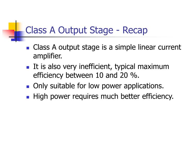
Class A Output Stage - Recap. Class A output stage is a simple linear current amplifier. It is also very inefficient, typical maximum efficiency between 10 and 20 %. Only suitable for low power applications. High power requires much better efficiency. Why is class A so inefficient ?.

E N D
Class A Output Stage - Recap • Class A output stage is a simple linear current amplifier. • It is also very inefficient, typical maximum efficiency between 10 and 20 %. • Only suitable for low power applications. • High power requires much better efficiency.
Why is class A so inefficient ? • Single transistor can only conduct in one direction. • D.C. bias current is needed to cope with negative going signals. • 75 % (or more) of the supplied power is dissipated by d.c. • Solution : eliminate the bias current.
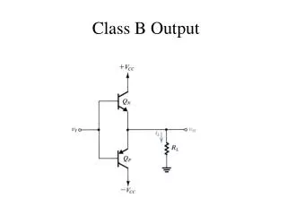
Class B Output Stage • Q1 and Q2 form two unbiased emitter followers • Q1 only conducts when the input is positive • Q2 only conducts when the input is negative • Conduction angle is, therefore, 180° • When the input is zero, neither conducts • i.e. the quiescent power dissipation is zero
Class B Current Waveforms Iout time IC1 time IC2 time
IC1 A/RL 0 p 2p Phase, q Class B Efficiency Average power drawn from the positive supply: A sin(q)
Load power: Efficiency: By symmetry, power drawn from +ve and –ve supplies will be the same. Total power, therefore:
Power Dissipation To select appropriate output transistors, the maximum power dissipation must be calculated. Just need to find the maximum value of PD to select transistors/heatsinks
E.g. VS = 15 V, RL = 100 W 1.5 PL PS PD 1 Power [W] 0.5 0 0 5 10 15 Peak Output Amplitude, A [V]
maximum when: Maximum Power Dissipation PD is a quadratic function of A,
Efficiency / Power Dissipation • Peak efficiency of the class B output stage is 78.5 %, much higher than class A. • Unlike class A, power dissipation varies with output amplitude. • Remember, there are two output devices so the power dissipation is shared between them.
Design Example Design a class B amplifier which will deliver up to 25 W into a 4 W load. Supply voltages must be larger than Amax so choose Vs = 15V.
But, with qJC = 1.92 °C/W Each of the two output transistors must be able to safely dissipate up to 5.7 Watts. Using a TIP120 & TIP 125: i.e. Either two heatsinks rated at less than 20°C/W are required or a single heatsink rated at less than 10°C/W.
Suggested heatsink Dimensions, 50mm x 50mm x 9.5mm Accommodates two devices Rating 6.5°C/W Cost 60p inc VAT
Cross-Over Distortion • A small base-emitter voltage is needed to turn on a transistor • Q1 actually only conducts when vin > 0.7 V • Q2 actually only conducts when vin < -0.7 V • When 0.7 > vin > -0.7, nothing conducts and the output is zero. • i.e. the input-output relationship is not at all linear.
Actual Input-Output Curve vout -VBE vin +VBE
Audio Demo Undistorted original Class B amplifier output
Class B Summary • A class B output stage can be far more efficient than a class A stage (78.5 % maximum efficiency compared with 25 %). • It also requires twice as many output transistors… • …and it isn’t very linear; cross-over distortion can be significant.