Download
1 / 35
350 likes | 481 Views
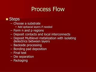
1. The Process flow for fabrication the resister IC. Step I: The Beginning-Choosing a substrate Before actual wafer fabrication, we must choose the starting wafers. The major choices are the type (N or P), resistivity, and orientation.

E N D
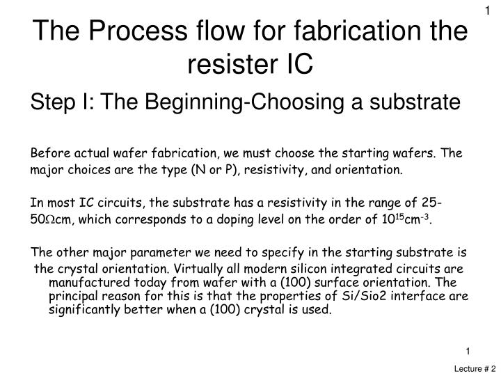
1 The Process flow for fabrication the resister IC Step I: The Beginning-Choosing a substrate Before actual wafer fabrication, we must choose the starting wafers. The major choices are the type (N or P), resistivity, and orientation. In most IC circuits, the substrate has a resistivity in the range of 25- 50cm, which corresponds to a doping level on the order of 1015cm-3. The other major parameter we need to specify in the starting substrate is the crystal orientation. Virtually all modern silicon integrated circuits are manufactured today from wafer with a (100) surface orientation. The principal reason for this is that the properties of Si/Sio2 interface are significantly better when a (100) crystal is used. Lecture # 2
3SiH4+4NH3Si3N4+12H2 Silicon nitride form a barrier against the impurities moving toward the Si surface.
4 Photolithography • In order to transfer resister information from the design to the wafer, a process known as photolithography is used. • For this process a material known as photoresist is first spread on the wafer. It is usually baked at about 100oC in order to drive off • solvants from the layer (photolithographic process will be covered in chapter 5 through. Lecture # 2
P Well Formation 1016 -1017 cm-3
High temperature Drive-In 2-3 micron
NMOS gate formation and adjusting VTH The single most important parameter in the both NMOS and PMOS devices is the threshold voltage To adjust VTH , two terms that are important are the doping concentration and the oxide capacitance.
Regrown of gate oxide Why oxide layer is stripped and then regrown?
Deposition of polysilicon layer SiH4 Si+2H2 Low ploy sheet resistivity and low gate resistance is required.
Selective Etching: to locate MOS gates Selectivity and anisotropy are big deal hare
High temperature Drive-In TED is a big issue hare!
8 Basic NMOS process flowchart. Lecture # 2
9 Basic bipolar process flowchart. Lecture # 2