Download
1 / 31
310 likes | 429 Views
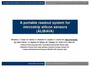
A readout system for microstrip silicon sensors (ALIBAVA). Marco-Hernández, R. a , Bernabeu, J. a , Casse, G. b , García, C. a , Greenall, A. b , Lacasta, C. a , Lozano, M. c , Martí i García, S. a , Martinez, R. c , Miñano, M. a , Pellegrini, G. c , Smith, N. A. b , Ullán, M. c

E N D
A readout system for microstrip silicon sensors(ALIBAVA) Marco-Hernández, R.a, Bernabeu, J.a, Casse, G.b, García, C.a, Greenall, A.b, Lacasta, C.a, Lozano, M.c, Martí i García, S.a, Martinez, R.c, Miñano, M.a, Pellegrini, G.c, Smith, N. A.b, Ullán, M.c a Instituto de Física Corpuscular (IFIC), Universidad de Valencia-CSIC,Valencia, Spain. b Department of Physics, Oliver Lodge Laboratory, University of Liverpool, Liverpool, UK. c Instituto de Microelectrónica de Barcelona, IMB-CNM, CSIC, Barcelona, Spain 10th RD50 Workshop, 2-6 June 2007, Vilnius, Lithuania
10th RD50 Workshop, 2-6 June 2007, Vilnius, Lithuania 2 OUTLINE • Introduction: • Motivations. • System requirements. • System architecture. • Daughter board: • Block diagram. • Readout chip main characteristics. • Fanins design • Mother board: • Block diagram. • FPGA block diagram. • System functionality: system states diagram. • PC Software. • System status. • Conclusion and outlook.
10th RD50 Workshop, 2-6 June 2007, Vilnius, Lithuania 3 MOTIVATIONS • Need of studying the main properties of highly irradiatedmicrostrip silicon sensors (SLHC). • Particularly the collected charge: detector performance. • Difficulty for obtaining this type of measurements: • Required equipment is expensive. • A large number of channels has to be measured. • Minimum standardization: often the same functions are required (amp. & s.c., ADC, temporal logic, PC communication) but implemented with different modules (NIM, CAMAC, VME or custom electronic modules). • Testing with an electronic system as similar as possible to those used at LHC experiments: a LHC front end readout chip should be used. • Analogue readout is preferred for pulse shape reconstruction.
10th RD50 Workshop, 2-6 June 2007, Vilnius, Lithuania 4 SYSTEM REQUIREMENTS • The system will be compact and portable. • The system will be used with two different laboratory setups: • It will have an external trigger input from one or two photomultipliers (radioactive source). • A synchronized external trigger output for pulsing an external excitation source (laser system). • The system will contain two front-end readout chips (Beetle, LHCb) to acquire the detector signals. • It will be communicated with a PC via USB, which will store and will process the data acquired. • The system will be controlled from a PC software application in communication with a FPGA which will interpret and will execute the orders. • The system will have its own supply system (from AC mains).
10th RD50 Workshop, 2-6 June 2007, Vilnius, Lithuania 5 SYSTEM REQUIREMENTS • Compact and portable system. • The system will be used with two different laboratory setups: • It will have an external trigger input from one or two photomultipliers (radioactive source). • A synchronized external trigger output for pulsing an external excitation source (laser system). • The system will contain two front-end readout chips (Beetle, LHCb) to acquire the detector signals. • It will be communicated with a PC via USB, which will store and will process the data acquired. • The system will be controlled from a PC software application in communication with a FPGA which will interpret and will execute the orders. • The system will have its own supply system (from AC mains). The main goal is reconstructing the analogue pulse shape at the readoutchipfront end with the highest fidelity from the acquired data.
10th RD50 Workshop, 2-6 June 2007, Vilnius, Lithuania 6 SYSTEM ARCHITECTURE • Two main parts: software part (PC) and hardware part. • Hardware part: a dual board based system. • Mother board intended: • To process the analogue data that comes from the readout chips. • To process the trigger input signal in case of radioactive source setup or to generate a trigger signal if a laser setup is used. • To control the hardware part. • To communicate with a PC via USB. • Daughter board : • It will be a small board. • It will contain two Beetle readout chips • It will have fan-ins and detector support to interface the sensors. • Software part: • It will control the whole system (configuration, calibration and acquisition). • It will generate an output file for further data processing.
10th RD50 Workshop, 2-6 June 2007, Vilnius, Lithuania 7 DB: BLOCK DIAGRAM
10th RD50 Workshop, 2-6 June 2007, Vilnius, Lithuania 8 BEETLE CHIP • Readout chip developed at ASIC laboratory of the University of Heildelberg. • Front-end output signal: this is the signal that will be reconstructed from analogue readout onto one port. • This signal is sampled into the analogue pipeline (128x187 cells) with the frequency of the Beetle chip clock (40 MHz). • Vp = kQ. Tp~ 25ns. Total pulse length about 65-70 ns. • The analogue pipeline programmable latency will be fixed to 128 CLK cycles (3.2 µs). • The TRIGGER signal will have to be active 128 CLK cycles (3.2 µs) after a particular front-end signal point of interest has been sampled.
126 127 H15 0 1 H0 100 ns 25 ns 143 x 25 ns = 3575 ns 10th RD50 Workshop, 2-6 June 2007, Vilnius, Lithuania 9 BEETLE OUTPUT FORMAT • Analogue output format: single readout. • Readout: 16 bits header + 128 analogue multeplexed channels. • Channel width of 25 ns. • Datavalid signal for readout detection.
10th RD50 Workshop, 2-6 June 2007, Vilnius, Lithuania 10 BEETLE OUTPUT FORMAT • Output dynamic range: ±66000 e- ~ ±500mV.
Daughter board Fan_chip Fan_int Fan_det Beetle DET 10th RD50 Workshop, 2-6 June 2007, Vilnius, Lithuania 11 S Beetle DET Detector board Bonding pads 80 um pitch, not staggered. 10 rows for multiple wire bonding FANINS DESIGN
10th RD50 Workshop, 2-6 June 2007, Vilnius, Lithuania 12 MB: BLOCK DIAGRAM
10th RD50 Workshop, 2-6 June 2007, Vilnius, Lithuania 13 SIGNAL CONDITIONING/ADC • The signal conditioning block is intended for transforming the differential voltage analogue input signal in order to: • Drive an oscilloscope which requires a single ended signal. • Drive an analogue to digital converter (ADC) which requires a differential input shifted signal. • ADC (one for each Beetle if parallel configuration): • 10 bit flash type with a sample rate of 40 MHz (MAX1448). • Nominal resolution of 2 mV (output signed code, 9 bits plus 1 sign bit). • Dynamic range will be ±512 mV.
10th RD50 Workshop, 2-6 June 2007, Vilnius, Lithuania 14 TRIGGER CONDITIONING-TDC • In case of radioactive source setup for obtaining a time stamp of each trigger. • Trigger conditioning: • Leading-edge discrimination of photomultiplier input signals. • Level conversion for an auxiliary signal. • Two dual LVPECL high speed comparators (MAX9601). • Four programmable voltage thresholds: generated with a quad 12 bits DAC (DAC7614). • TDC: • A TDC integrated circuit (TDC-GP1). • Nominal resolution: 600 ps. • 100 ns dynamic range. • Retrigger mode capability.
10th RD50 Workshop, 2-6 June 2007, Vilnius, Lithuania 15 TRIGGER OUTPUT • In case of laser setup. • A synchronised trigger signal (TRIG OUT) will be generated to drive a laser source so that the pulse shape can be reconstructed. • Programmable delay circuit (3D7428): • Resolution: 1 ns. • Range: up to 255 ns. • Programmed by FPGA by serial interface. • Following this block a 50 Ω driver will be incorporated for driving a pulse generator input.
10th RD50 Workshop, 2-6 June 2007, Vilnius, Lithuania 16 OTHER BLOCKS • SDRAM (256 Mb): for acquisition data storage. • SLOW CONTROL: generated directly by the FPGA. External pullup resistors for SDA and SCL lines. • FAST CONTROL: • LVDS driver (DS90LV47A) and LVDS receiver (DS90LV48A). • Six CM noise suppressor chokes (23Z105SM). • USB: USB controller (FT245R) for USB to FIFO parallel (8 bits) bidirectional data transfer. • SUPPLY SYSTEM: • DC input from AC adapter. • Digital levels from 2 DC-DC converter + 1 linear regulator. • Analogue levels from DC-DC converter + 1 linear regulator. • Daugther board level from DC-DC converter.
10th RD50 Workshop, 2-6 June 2007, Vilnius, Lithuania 17 FPGA: BLOCK DIAGRAM • Xilinx Spartan-3 clocked at 40 MHz.
10th RD50 Workshop, 2-6 June 2007, Vilnius, Lithuania 18 FPGA: BLOCK DIAGRAM • CFSM and SDRAM Control implemented with a microblaze embedded processor.
10th RD50 Workshop, 2-6 June 2007, Vilnius, Lithuania 19 CFSM STATE DIAGRAM • Possible system states.
10th RD50 Workshop, 2-6 June 2007, Vilnius, Lithuania 20 PC SOFTWARE • Requirements: • Control the whole system (configuration, calibration and acquisition). • User interface with the system (GUI). • Generation of information (output file). • Two software levels: • Low level: software/mother board communication by USB (no driver design required: VCP or D2XX from USB controller). • High level: GUI and output file generation. • Programming language: C/C++ • Implemented with ROOT framework. • Operating system compatibility: Linux and Windows. • An “emulator” of the sytem (FPGA reduced firmware) has been implemented with a FPGA development board and USB controller board for low level software development.
10th RD50 Workshop, 2-6 June 2007, Vilnius, Lithuania 21 PC SOFTWARE • Picture of the FPGA development board and the USB expansion board: USB Expansion Board
10th RD50 Workshop, 2-6 June 2007, Vilnius, Lithuania 22 SYSTEM STATUS • A prototype of the system is being developed. • Daughter board: • 20 PCBs already produced. • Currently, one of them it is being populated for testing the system. • Fan-ins already designed and produced. • Mother board: • First PCB prototype already produced and partially populated for testing the system. • FPGA firmware finished for laser setup. Two blocks are being developed for radioactive source setup (TDC Control and DAC Control). The rest of FPGA blocks have been developed. • Power supply, SDRAM, USB controller, FPGA hardware and FPGA firmware structure already tested and working as expected. • PC software: • Presently, it is being developed and it is almost finished. • When finished will be used for testing, up to now Matlab it is being used for testing the mother board.
10th RD50 Workshop, 2-6 June 2007, Vilnius, Lithuania 23 SYSTEM STATUS • Picture of a daugther board partially populated.
10th RD50 Workshop, 2-6 June 2007, Vilnius, Lithuania 24 SYSTEM STATUS • Current state of the motherboard prototype.
10th RD50 Workshop, 2-6 June 2007, Vilnius, Lithuania 25 SYSTEM STATUS • Current state of the motherboard prototype. Power Supply
10th RD50 Workshop, 2-6 June 2007, Vilnius, Lithuania 26 SYSTEM STATUS • Current state of the motherboard prototype. FPGA Block
10th RD50 Workshop, 2-6 June 2007, Vilnius, Lithuania 27 SYSTEM STATUS • Current state of the motherboard prototype. USB Block
10th RD50 Workshop, 2-6 June 2007, Vilnius, Lithuania 28 SYSTEM STATUS • Current state of the motherboard prototype. SDRAM Block
10th RD50 Workshop, 2-6 June 2007, Vilnius, Lithuania 29 SYSTEM STATUS • Current state of the motherboard prototype. Trigger out Block (Laser setup)
10th RD50 Workshop, 2-6 June 2007, Vilnius, Lithuania 30 CONCLUSION AND OUTLOOK • A readout system for microstrip silicon sensors is being developed. • A daughter board prototype and a mother board prototype have been produced. • PC software is being developed and almost finished. • These prototypes and the PC software are currently being tested separately. • From next week, the mother board, the daughter board and the PC software will be used together for testing the system. • The main aim is being able to use the system with the laser setup. • Then, it is expected to be able to use the system with radioactive source setup.
A readout system for microstrip silicon sensors(ALIBAVA) Marco-Hernández, R.a, Bernabeu, J.a, Casse, G.b, García, C.a, Greenall, A.b, Lacasta, C.a, Lozano, M.c, Martí i García, S.a, Martinez, R.c, Miñano, M.a, Pellegrini, G.c, Smith, N. A.b, Ullán, M.c a Instituto de Física Corpuscular (IFIC), Universidad de Valencia-CSIC,Valencia, Spain. b Department of Physics, Oliver Lodge Laboratory, University of Liverpool, Liverpool, UK. c Instituto de Microelectrónica de Barcelona, IMB-CNM, CSIC, Barcelona, Spain 10th RD50 Workshop, 2-6 June 2007, Vilnius, Lithuania