Download
1 / 44
530 likes | 937 Views
Electronic circuit design and component selection. Nan-Wei Gong MIT Media Lab MAS.S63: Design for DIY Manufacturing. Goal for today’s lecture. Pick up proper components for your project Rule of thumb for PCB design Suggestions for PCB layout and manufacturing

E N D
Electronic circuit design and component selection Nan-Wei Gong MIT Media Lab MAS.S63: Design for DIY Manufacturing
Goal for today’s lecture • Pick up proper components for your project • Rule of thumb for PCB design • Suggestions for PCB layout and manufacturing • Soldering and de-soldering basics • Small - medium quantity electronics project production • Homework : Design a PCB for your project with a BOM (bill of materials) and estimate the cost for making 100 (PCB manufacturing + assembly+ components)
Design Process Test Circuit Component Selection PCB Design PCB Manufacturing Component Placement
Design Process • Test circuit – bread boarding/ buy development tools (breakout boards) / simulation • Component Selection– spec / size / availability (inventory! Need 10% more parts for pick and place machine) • PCB Design– power/ground, signal traces, trace width, test points / extra via, pads / mount holes, big before small • PCB Manufacturing – price-time trade-off/ • Place Components – first step (check power/ground) -- work flow
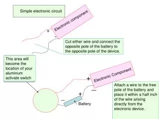
Test Circuit Construction Breadboard + through hole components + Breakout boards, surfboards + hookup wires Breakout boards Surfboard : surface-mount to through hole Dual in-line (DIP) packaging http://www.beldynsys.com/cc521.htm Source : http://en.wikipedia.org/wiki/File:Breadboard_counter.jpg
Development Boards – good reference for circuit design and component selection Sometimes, it can be cheaper to pair your design with a development board for your “product” if you are only manufacturing in a small quantity..
Simulate you (analog) circuit if needed! http://www.ecircuitcenter.com/ https://www.circuitlab.com/ http://phet.colorado.edu/en/simulation/ http://www.openmusiclabs.com/testpage/ http://www.daycounter.com/ …and more!
Design Process • Test circuit – bread boarding/ buy development tools (breakout boards) / simulation • Component Selection– spec / size / availability (inventory! Need 10% more parts for pick and place machine) • PCB Design– power/ground, signal traces, trace width, test points / extra via, pads / mount holes, big before small • PCB Manufacturing – price-time trade-off/ • Place Components – first step (check power/ground) -- work flow
Electronic Components Distributor Components
Wire Selection • WIRE GAUGE – AWG (American wire gauge) • the diameters of round, solid, nonferrous, electrically conducting wire. The cross-sectional area of each gauge is an important factor for determining its current-carrying capacity. • JACKET (Insulation) • The jacket physically protects the internal components of a cable, improves the cable’s appearance and provides flame retardancy –Protects from the environment–Protects from the rigors of installation http://www.belden.com/docs/upload/Insulations-Jackets.pdf
Cabling Solid RF signals Stranded Coax - BNC Coax - SMA breadboard jumpers – 23 AWG on-board jumpers > 30 AMG Pre-crimped wire http://www.oregonrfid.biz/store/index.php?main_page=page&id=3 RG-59 CABLE A: outer plastic sheathB: woven copper shieldC: inner dielectric insulatorD: copper core Stranded wire is used when higher resistance to metal fatigue is required. Twisted Pair Flexible flat cable (FFC) Ribbon two conductors (the forward and return conductors of a single circuit) are twisted together for the purposes of canceling out electromagnetic interference (EMI) from external sources http://www.asiconnectors.com/member/x964-Flexible-Flat-Cable-Connectors.asp
Antenna for Zigbee Radio ¼ wavelength solid 23 AWG wire Jumpers between chips 30 AWG solid wire Connector for flexible flat cable (for programmer)
Switches - mechanical or actuators DIP switch Tactile button SPST switch http://search.digikey.com/scripts/DkSearch/dksus.dll?x=0&y=0&lang=en&site=us&KeyWords=switch SPDT switch
Switches http://en.wikipedia.org/wiki/Switch
Battery Three basic things - Cell Voltage, Load Current, Amp-Hour (symbol Ah, AHr, A·h, A h) http://www.rfcafe.com/references/electrical/batteries.htm
Footprint - same component / IC comes in different footprints
Flat Chips - Capacitors and Resistors How to read the value :
Capacitors Voltage rating for capacitors – Really important for power circuits http://www.bcae1.com/capacitr.htm http://en.wikipedia.org/wiki/File:Cap-elko-smd-polarity.jpg
Footprint - same IC comes in different footprints SMD (surface-mount device) ICs http://www.topline.tv/SMDnomen.pdf Courtesy of Analog Device’s poster
SOIC (Small Outline Integrated Circuit) SMD leads styles http://www.topline.tv/SMDnomen.pdf
PCB design software Free software EAGLE (Easily Applicable Graphical Layout Editor) http://www.cadsoftusa.com/ http://www.sparkfun.com/tutorials/109 Tutorials from Sparkfun -> • Two major components • Schematics • PCB Layout • And sometimes.. 3D simulation http://www.freepcb.com/ http://www.expresspcb.com/ http://www.4pcb.com/free-pcb-layout-software/ And more… But it’s just another CAD software
PCB design software Things you need to know Pick your software (we will have a tutorial on EAGLE) Pick the parts build “footprint” for the parts, or find them from a library Draw circuit diagram Schematics Route the physical circuitry PCB Layout
Things you need to know Pick your software (we will have a tutorial on EAGLE) Pick the parts build “footprint” for the parts, or find them from a library Draw circuit diagram Schematics Route the physical circuitry PCB Layout Create PCB file from schematics Design schematics with components from a library
Things you need to know Pick your software (we will have a tutorial on EAGLE) Pick the parts build “footprint” for the parts, or find them from a library Draw circuit diagram Schematics Route the physical circuitry PCB Layout Tips - right click to switch through routing menu middle click to switch between layers
PCB design rule of thumb • Trace width for signal and power lines • When placing narrow traces, 0.012" or less, avoid sharp right angle turns, use 45 or 135 degree turns. The problem here is that in the board manufacturing process, the outside corner can be etched a little more narrowand causes transmission reflections. • Power trace width depending on the current • Noise reduction • Decoupling capacitors • Analog/Digital trace placement • Via and mount holes
Trace width calculation – to avoid voltage drop (trace resistance) and over heating Area[mils^2] = (I[Amps]/(k*(Temp_Rise[deg. C])^b))^(1/c) Then, the Width is calculated: Width[mils] = Area[mils^2]/(Thickness[oz]*1.378[mils/oz]) http://circuitcalculator.com/wordpress/2006/01/31/pcb-trace-width-calculator/
Constructing Your Power Supply- Layout Considerations http://www.ti.com/lit/ml/slup230/slup230.pdf
Split Ground Planes 0 Ohm resistor or simple connect them with trace Analog ground Digital ground Ferrite Bead Split Power Planes A ferrite bead is a passive electric component used to suppress high frequency noise in electronic circuits It employ high dissipation of high frequency currents in a ferrite to build high frequency noise suppression devices http://en.wikipedia.org/wiki/Ferrite_bead Power Plane Power Plane (switching supply / Clock)
Decoupling • http://en.wikipedia.org/wiki/Decoupling_capacitor • Decoupling is the process of adding small LC networks to ICs to provide a • low impedance to ground at high frequencies and surge current at • switching frequencies.
The basic layers are: copper, silk screen, solder mask, and NC Drill.Copper layer stands for the conductive wires, silk screen is the marks andnames, solder mask(stop layer)is the top non-conductive layer,and NC drill is the drill hole location.For example, if you need a two layer PCB with top layer silk screen, you willneed to send • Top Copper (GTL) • Top Solder mask (GTS) • Top Silkscreen (GTO) • Bottom Copper (GBL) • Bottom Solder mask (GBS) • Bottom Silkscreen (GBO) • Drill File
Top Copper Top Solder mask Top Silkscreen Bottom Solder mask Bottom Copper Bottom Silkscreen
PCB Assembly • Things you need to know • Soldering • De-soldering • Re-flow • Pick and Place Machine
Soldering • Solder size • Depending of size of the part • Solder paste • For SMD components • Solder tips http://store.curiousinventor.com/guides/Surface_Mount_Soldering/Tools/
De-soldering and Re-flow • Flux - chemical cleaning agent, flowing agent, or purifying agent • Solder Sucker or Solder-wick Before After Hot air station for removing quad flat packages (where there are too many leads to properly de-solder it without ) Infrared Rework Station Same idea with the hot air station, The only difference is it won’t blow away tiny parts
PCB manufacturing and assembly http://www.custompcb.com/starting at $18 eachhttp://www.advancedcircuits.com/$33/boardhttp://www.streamlinecircuits.com/Need to know • Board layers • Material (FR4) • Trace width • Solder mask and silkscreen color • Thickness
PCB Design cost calculator - http://www.ladyada.net/library/pcb/costcalc.html
Cheap way to test your circuit design – barebones PCB without solder mask Cheap way to get more boards made from the same order Put via everywhere so you can separate different designs! Break the board with a bender
Board assembly • http://www.protoexpress.com/ • http://www.advancedcircuits.com/ • http://www.spinpcb.com/ • http://www.leaflabs.com • http://www.suntroncorp.com • http://www.rapidboard.com/ • http://www.pcacorporation.com/ • http://www.pcbassemblydepot.com/ • http://www.flexone.com/ INFO needed for a quote - - Board quantity - Unique parts - Both Sides? - Lead-free? - # of SMT parts - # of through hole - # of fine pitch / QFM items - Jumper wire? (if you made mistakes)
How to order PCB assembly • You can ask them to order the parts or you can send them the parts. • Files needed - • Bill of Materials(BOM) • Centroid data • Centroid data (aka Insertion or Pick-and-place or XY data) - This is the machine file, which should include: X, Y, Theta, Side of Board (Top or Bottom), and Reference Designator. • The BOM from Eagle is not the format that they like. For generating Centroid data, seehttp://www.screamingcircuits.com/services/how-it-works.aspx#eagle