Download
1 / 23
230 likes | 321 Views
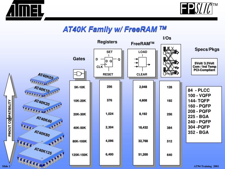
SET. D. Q. D. Q. CLK. RESET. 256 576 1,024 2,304 4,096 6,400. 5K-10K 10K-20K 20K-30K 40K-50K 80K-100K 125K-150K. PINOUT COMPATIBILITY. AT40K40. AT40K80. AT40K125. AT40K Family w/ FreeRAM TM. I/Os. Registers. FreeRAM TM. Specs/Pkgs. LOAD. Gates. 5Volt/ 3.3Volt

E N D
SET D Q D Q CLK RESET 256 576 1,024 2,304 4,096 6,400 5K-10K 10K-20K 20K-30K 40K-50K 80K-100K 125K-150K PINOUT COMPATIBILITY AT40K40 AT40K80 AT40K125 AT40K Family w/ FreeRAM TM I/Os Registers FreeRAMTM Specs/Pkgs LOAD Gates 5Volt/ 3.3Volt Com / Ind Temp PCI-Compliant CLEAR AT40K05 2,048 4,608 8,192 18,432 32,768 51,200 128 192 256 384 512 640 AT40K10 84 - PLCC 100 - VQFP 144- TQFP 160 - PQFP 208 - PQFP 225 - BGA 240 - PQFP 304 -PQFP 352 - BGA AT40K20
FPSLIC- Embedded FPGA Core • SRAM based technology • LUT cell based • Distributed SRAM blocks • FreeRamTm from 4.6K – 18.4K bits • Fully symmetrical architecture • Partial/Dynamic reconfiguration • Family of AT40K05/10/20/40 in production • for more than 3 years • Tools/application notes/ IPs available. Proven AT40K FPGA Technology
I/O Distributed FPGA RAM Interface to AVR and SRAM Core Cells Repeaters FPGA Core Overview >> Patented RAM can reduce FPGA size requirements by >50%
FPGA Cell to Bus Connections • Each Cell input can be • connected to a local bus • Each Cell output can be • connected to a local bus • 5 Local buses horizontally per • sector row • 5 local buses vertically per • sector column
Cell to Cell Direct Connections • Each Cell connects to 8 • nearest neighbors • Each Cell has 4 orthogonal • connections • Each Cell has 4 diagonal • connections
Ci Xi Pi Yi X3 X2 X1 X0 Y0 X3Y0 X2Y0 X1Y0 X0Y0 + Pi Ci Y1 X3Y1 X2Y1 X1Y1 X0Y1 Pi+1 Ci+1 Y2 X3Y3 X2Y2 X1Y2 X0Y2 Pi+1 Y3 X3Y3 X2Y3 X1Y3 X0Y3 Ci+1 P7 P6 P5 P4 P3 P2 P1 P0 Array Multipliers Parallel Multiplier Cell >> Key to High-Performance Processing
FPGA Core Cell "1" NW NE SE SW "1" "1" N S E W X W Y 1-X 2-Y 3-W Z(L) X(L) W(L) Y(L) a0 a1 a2 a2 a1 a0 8x1 LUT 8x1 LUT V1 V2 V3 V4 V5 out out "1" "0" "1" H1 H2 H3 H4 H5 Z 0 1 4-Z Feedback "1" OE OE H V 5-OE D CLOCK RESET or SET Q Cell Inputs Highlighted initalics X Y NW NE SE SW N E S W
Reg Reg Reg Sample AT40K Core Cell ‘Modes’ ‘Arithmetic’ Mode ‘Synthesis’ Mode A Sum A B B 3 LUT 4 LUT Logic Out CIN C D Carry 3 LUT Random Logic Full Adder/Counter ‘DSP’ Mode ‘Network’ Muxing Mode A A Carry B LUT 3 B OUT 2:1 MUX Select Product PPSI LUT 3 CIN Enable Switches Multiplier Cell
Atmel Diagonal direct connection cell cell CLB CLB cell cell CLB CLB AT40K Key Features DSP Xilinx 4K series requires 12 CLBs to create a 4 x 4 array multiplier. Each CLB is equivalent to 2 Atmel core cells which means a Xilinx 4 x 4 array multiplier is equivalent to 24 Atmel core cells. Xilinx does not have diagonal direct connects so they also consume a large number of bus resources to do multiplier. AT40K 4 X 4 array multiplier 16 core cells Atmel Features: Core cell ‘up-stream’ AND gate give 1 multiplier ‘tile’ per core cell. Diagonal and Orthogonal core cell connection mean no bussing resource consumed to make array multiplier Xilinx need two buses to make a Diagonal
Din Dout WAddr RAddr 32x4 RAM WE OE FPGA SRAM • 32 X 4 Ram in corner of each sector • Ram can be sync or async • Ram can be single or dual ported • Ram can be reset via configuration • Ram can operate at 100MHz • Data and address come from local • and express bus connections Dedicated SRAM routing resource
32x 4 bits of Dual port RAM AT40K Key Features FreeRAM Atmel Features: Distributed SRAM “FreeRAM” Fast 10ns access time Fully Programmable Single or Dual port Synch or Async Using RAM does not use core cells Xilinx 4K series has 16 x 1 Dual port Ram in each CLB 32 x 4 Dual port RAM is 8 CLBs and each Xilinx CLB is 2 X an Atmel core cell. A Xilinx 32 X 4 Dual port RAM consumes the equivalent of 16 Atmel core cells !!!! With AT40K the RAM is FREE
AT40K Clocking Scheme • Individual Clock per sector column • Clock and Clock BAR at sector boundary • Column Clock can be any one of 8 Global • clocks • Clock from Column Clock or Express Bus • 4 Fast Clocks (2 per side for PCI spec) • Low power tie-off
AT40K Reset Scheme • Individual reset per Sector column • Reset and Reset BAR • Any device pin can be designated as reset • Reset from Global Reset or Express Bus • Each D Flip-Flop can be Set or Reset
FPGA Primary I/O • I/O interfaces to core cell • I/O connects into repeaters • on row above and row • below • Programmable input delay • CMOS/TTL input levels • Pull-up or pull-down • resistor • Open source/drain output • System friendly bus keeper >> Supports Pin-Locking!
P P P P cell cell cell cell S S S S S P P P P P cell cell cell cell S S S S P P P P cell cell cell cell AT40K Key Features Pin Locking AT40K ‘Lock-it and Leave-it’tm I/O structure Unique I/O bus connections mean that pin locking problems are virtually eliminated 1 Primary I/O connects to 12 core cells & 1 Secondary I/O connects to 8 core cells
AT40K FPGA FPGA Designs Figaro IDS FPGA Development Tools AT17 • IDS supports Schematic, VHDL or Verilog Design Entry • It generates a BST file for programming the Configurator
FPGA HDLPlanner™ • HDLPlanner™ • Technology independent • design entry • Enhances design re-use • Shorter design cycle • Supports Verilog & VHDL • Syntax correct templates • Support for macro • generators • Context highlighting • Seamless interface to • synthesis • Integrate user defined • components • Knowledge archival
Push Button IP - Macro Generators • Macro Generators • Hard or Soft Layouts • Parameterizable • Auto HDL generation • Auto Schematic Generation • Auto Simulation Model • Power Calculation • Area Calculation • Post Layout Performance • Architecture Optimized • Open development lang.. • Auto insertion of pipelining • Supports Logic & Memory
Exemplar Leonardo Spectrum HDL Synthesis • Easy to use • Fast RTL Optimization • Produces the best results • Integrated RTL to P&R
ModelSim HDLSimulation • Committed to HDL Simulation Leadership • Quick Compilation • Fast Simulation • Ease-of-Use • Full debug at any level
FPSLIC-FPGA Development Software • FPGA Development Tools • Push Button 85%+ APR • XNF/EDF/WIR Import • Hierarchy Browser • Architecture Mapping • Multi-Chip Partitioning • Floor planner • Bitstream Utilities • Incremental Design Change • Export VHDL/Verilog netlists • Back Annotation support • Extensive interactive help.
FPSLIC-FPGA Development Software • FPGA Development Tools • User Library Management • Enhances Design re-use • Interactive Layout Editor • Timing Driven Design • Graphical Constraint Entry • Multi Cycle Clk Constraint • Async. Path Delay Constraint • Static Timing Analysis • Interactive Timing Analysis