Download
1 / 17
170 likes | 286 Views
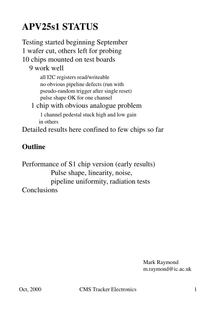
APV25s1 STATUS. Testing started beginning September 1 wafer cut, others left for probing 10 chips mounted on test boards 9 work well all I2C registers read/writeable no obvious pipeline defects (run with pseudo-random trigger after single reset)

E N D
APV25s1 STATUS Testing started beginning September 1 wafer cut, others left for probing 10 chips mounted on test boards 9 work well all I2C registers read/writeable no obvious pipeline defects (run with pseudo-random trigger after single reset) pulse shape OK for one channel 1 chip with obvious analogue problem 1 channel pedestal stuck high and low gain in others Detailed results here confined to few chips so far Outline Performance of S1 chip version (early results) Pulse shape, linearity, noise, pipeline uniformity, radiation tests Conclusions Mark Raymond m.raymond@ic.ac.uk CMS Tracker Electronics
Wafer layout ~ 390 viable APV25s1 sites / wafer CMS Tracker Electronics
Wafer detail showing reticule reticule consists of 4 APVs 1 APVMUX/PLL test structures CMS Tracker Electronics
APV25s1 layout 7.1 mm 8.1 mm design changes input edge layout changes to reduce track resistance (input pad layout changed) calibration capacitor layout improved gain increased (resistor values at mux input stage) added internal master current reference for bias generator (backend pad layout changed from s0 version) digital bug in pipeline logic fixed minor tweaks to component values to achieve greater margins for operation (shaper feedback resistance) CMS Tracker Electronics
Output data frame Raw data frame Digital header 1 mip Current [mA] Analogue part of data frame software reordered Actual channel order Samples at 50 nsec. intervals differential current output (+ve o/p only shown above) nominal (mid-range) gain now 1.2 mA/mip variable between 0.8 and 1.5 in 5 steps CMS Tracker Electronics
APV25s1 biasing internal/external option determined by 2 pads (IREF & IREFBIAS) mode IREF IREFBIAS IVDD[mA] IVSS[mA] external 128mA (R to VDD) VDD 94 156 internal disconnect GND 89 143 (VDD=2.5, GND=1.25, VSS=0) recommended bias settings (decimal) (preliminary) if external bias at 128 mA IPRE 85 IPCASC 45 IPSF 30 ISHA ~ 30 tune for optimum pulse rise time ISSF 30 IPSP 48 IMUXIN 30 VFP ~ 30 VFS ~ 60 tune for optimum pulse fall time NOTE: These current values are ~70% less than those for s0 (current mirroring ratio changed) CMS Tracker Electronics
Pulse shape dependence on input capacitance ADC units time [nsec.] Peak mode pulse shape tuned (shaper amplifier bias settings) for each value of input capacitance ISHA: 21 -> 65 (I2C register setting ~ roughly = mA) VFS: 63 -> 50 CMS Tracker Electronics
Pulse shape dependence on shaper feedback resistor control voltage VFS Feedback FET length slightly reduced from S0 version to ensure short enough time constant achievable with margin optimum value here ~ 60 (decimal) CMS Tracker Electronics
Linearity Input signal charge injected in 0.5 mip steps from 0.5 to 7 mips. ADC units time [nsec.] output signal [mips] input signal injected [mips] output normalised to input at 1 mip point linearity good up to 3 mips, gradual fall off beyond CMS Tracker Electronics
Gain/calibration uniformity Calibration capacitor layout improved Calibration response of all 128 channels superimposed ADC units 3.125 nsec steps Pulse peak height dependence on channel number frequency ADC units channel no.(mux order) peak ht. [ADC units] Good channel matching CMS Tracker Electronics
Noise Dependence on input capacitance ENC [rms electrons] Input capacitance [pF] No dependence on channel number < 2000 electrons achievable for detectors < 25 pF CMS Tracker Electronics
Pipeline - pedestals Pedestal dependence on pipeline location channel 19, peak mode ADC units pipeline location Measure for every channel, take rms value, convert to electrons and histogram frequency rms electrons No significant noise contribution CMS Tracker Electronics
Pipeline – gain uniformity How well do pipeline capacitors match? Signal retrieved as charge so mismatch => gain dependence on pipeline capacitance Measure by storing/retrieving signal to/from every cell frequency ADC units Very good matching between pipeline cells CMS Tracker Electronics
Radiation tests 1chip irradiated to 10 Mrads using 50 kV X-rays before after 10 Mrads ADC units time [nsec.] minor retuning of pulse shape required after irradiation Noise – histogram all channels before after 10 Mrads rms ADC units Almost no observable degradation after 10 Mrads (confirms results from s0 run) CMS Tracker Electronics
Probe testing plans for APV25s1 New probe card made (only needs active and decoupling components to be added) similar (functionally) to s0 version except multiple (3) probes for power on front edge 1 amplifier input probed allowing true chip gain to be determined Additions to test software measure pulse height for probed channel test multi-mode operation sweep one bias setting measuring power supply currents Tested die should be available early November CMS Tracker Electronics
APVMUX/PLL status CMS Tracker Electronics
Conclusions Early APV25s1 results indicate good performance consistent with results from APV25s0. Minor problems fixed. CMS Tracker Electronics