Download
1 / 26
260 likes | 340 Views
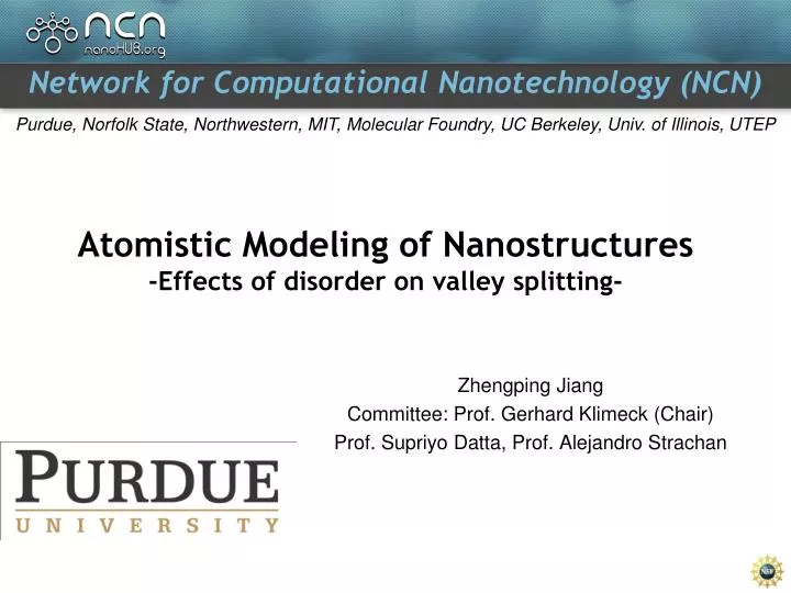
Atomistic Modeling of Nanostructures -Effects of disorder on valley splitting-. Zhengping Jiang Committee: Prof. Gerhard Klimeck (Chair) Prof. Supriyo Datta, Prof. Alejandro Strachan. Nanoelectronic Device Scaling. Future? 2^n*2G. PC 2G 2008. Laptop 2*2G 2009. PC 4*2G 2010.

E N D
Atomistic Modeling of Nanostructures-Effects of disorder on valley splitting- Zhengping Jiang Committee: Prof. Gerhard Klimeck (Chair) Prof. Supriyo Datta, Prof. Alejandro Strachan
Nanoelectronic Device Scaling Future? 2^n*2G PC 2G 2008 Laptop 2*2G 2009 PC 4*2G 2010 Technology makes life simple, not heavy. • One bit, typically: • DRAM: MOS transistor + capacitor Future: More info in one memory unit or decrease size. Acknowledgement: Robert Chau, Intel MOS: ~60nm with pitch 2
Why quantum computation is pursued? Concept of Quantum computation: Electrical engineer bit 1 0 Can we realize it? qubit a|1>+b|0> Spin ! Computer science Is it small? Physicist Logician … comparable or even smaller than DRAM More information in one qubit! What are we waiting for? 3
Challenge to realize qubit Quantum computing dilemma: Manipulate qubit by external force. Isolation from external force to maintain quantum information between gate operations. Which material could be used? • silicon • Closest to mainstream semiconductor technology. • Long spin coherence time. Existence of spin‐free nuclear isotopes. • Valley degeneracy could be problem in qubit operation. Valley degeneracy is potential source for decoherence.* To use silicon, degeneracy must be lifted. *B. Koiller et al. PRL 88 (2002) 4
kz kz ky ky kx kx QW Valley-splitting valley splitting – lift valley degeneracy Biaxial strain splits six-fold* valley-degeneracy into • Lower two-fold degeneracy • Higher four-fold degeneracy How to lift valley degeneracy? • Lowest two-fold degenerate valleys split • in the presence of sharp confinement • potentials in QWs. 4 fold Energy spacing between two resulting energy level. 6 fold 2 fold • Valley-splitting is a critical design parameter for QC devices. • -> remove degeneracy. *Spin degeneracy is not included here. 5
2nd 1st 1st quantize k E 2 propagating states Parabolic Dispersion 1 boundstate k Simple quantum well states Most basic quantum mechanical problem: Particle in a box 2nd L Schrödinger Equation 6 Thanks to Neerav for figures.
2nd 1st E k1,2=/L k1,2=/L k Valley splitting: Quantum WellsSpecial Considerations in Si 2 valleys 4 propagating states 2 bound states k1,2 envelope km fast oscillations T. Boykin et al. PRB 70 (2004) 7
Can we build QC now? Valley splitting E3 Valley + spin splitting Valley + spin splitting E2 Valley splitting E1 QC states E0 QC states • Quantum computation requirements: • 2 level system: spin degree of freedom. • Non-degenerate state well separated from excited states. 2 fold • Insufficient valley splitting: • Interaction with environment destroy origin phase of states. • Error when reading out states. Sufficient valley splitting is required to preserve quantum information. 8
Realization of a Si based QC architecture SiGe Si Alloy disorder Quantum Computing devices Friesen et al., PRB, 2003 Goswami et al., Nature Physics, 2007 Why choose SiGe: SiGe substrate provide tensile strain to Si, which lifts degeneracy (6 to 2). Relaxed SiGe confines electron in Si. (2 to 1) Confinement potential and strain could be tuned by Ge composition, which could be used to control valley splitting. Disorder in alloy must be considered! Kharche et al., APL., 2007 9
Realization of a Si based QC architecture SiGe Si Alloy disorder Quantum Computing devices Friesen et al., PRB, 2003 • Quantities show potential effects: • Electric field: top and back gate • Strain: SiGe lattice mismatch • Well width • Barrier disorder Understand effects of these quantities and find a effective simulation model. Kharche et al., APL., 2007 10
Simulation results Valley splitting in (100) SiGe/Si/SiGe • Approaches • Electric field and well width dependence • QW with no disorder barrier • QW with SiGe barrier Dependence of VS on barrier disorder • Approaches • Disorder effects • Ordered barrier and random alloy barrer • Ordered barrier and partially ordered barrier 11
Valley splitting in (100) SiGe/Si/SiGe QW Objective: • Modeling real strain in Si QW. • Modeling valley splitting in quantum well structure with SiGe barrier. Method: • Strain: VFF Keating model • Bandstructure: Nearest neighbor sp3d5s* tight - binding model Results: • Experimental observed tri-mode bond length distribution. Lattice mismatch Increase SiGe volume in strain calculation to mimic relaxed SiGe substrate and strained Si Bond length changes with Ge composition but tends to preserve their bulk value. 12
Valley splitting in (100) SiGe/Si/SiGe QW Smooth VS variation with electric field Objective: • Valley splitting dependence on well width with smooth barrier.(no SiGe) • Valley splitting dependence on electric field. Method: • Strain: VFF Keating model • Bandstructure: Nearest neighbor sp3d5s* tight - binding model • Smooth barrier simulated by carbon TB parameters. Results: • Strong oscillation with well width in flat QW. • Suppression of oscillation in electric field. no disorder Boykin et al., APL. 2004 E Effective W not change WF confinement 13
Valley splitting in (100) SiGe/Si/SiGe QW Objective: • VS dependence on well width with disorder barrier. • Match VS with experimental width and electric field. • 2MV/m electric field • Si well thickness: 3.8~20nm Method: • Strain: VFF Keating model • Bandstructure: Nearest neighbor sp3d5s* tight - binding model Results: • Qualitative agreement with experiments.(trend & error) • Disorder mixes valley splitting values for thin QWs. Exp. Data Exp: At 2MV/m, well width did not change for W>9nm* *K. Sasaki, APL (2009) 14
Valley splitting in (100) SiGe/Si/SiGe QW Objective: • VS dependence on electric field. • Predict VS in high electric field. Method: • Strain: VFF Keating model • Bandstructure: Nearest neighbor sp3d5s* tight - binding model Results: • Uncertainty due to disorder is huge in high field. • In contrast to smooth barrier simulation: • Electric field != smooth VS variation • High electric field: • WF is pushed to interface. • Strong alloy scattering. • Uncertainty due to disorder 15
Simulation results Valley splitting in (100) SiGe/Si/SiGe • Approaches • Electric field and well width dependence • QW with no disorder barrier • QW with SiGe barrier Dependence of VS on barrier disorder • Approaches • Disorder effects • Ordered barrier and random alloy barrer • Ordered barrier and partially ordered barrier 16
dependence of VS on barrier disorder Objective: • Understand how disorder affects VS. • Effects of different bonds in VS. Method: • Strain: VFF Keating model • Bandstructure: Nearest neighbor sp3d5s* tight - binding model • Geometry construction powered by atomistic modeling Example: • 25% atom replaced by Ge • Ge disconnected cell • Ge adjacent cell (b) (a) Replace #4 and #6. Only Si-Ge bond exist. Replace #2 and #6. Si-Ge and Ge-Ge bond in crystal. 17
dependence of VS on barrier disorder Objective: • Understand how disorder affects VS. • Effects of different bonds in VS. Method: • Strain: VFF Keating model • Bandstructure: Nearest neighbor sp3d5s* tight - binding model • Geometry construction powered by atomistic modeling Results: • Different bond types have different effects on VS. • Different bonds show different scattering potential for electrons.* • Notes: • Build barrier with one cell type • -> ordered barrier • Random place Ge in barrier • -> disorder barrier (# in fig.: Ge atom position) Saumitra etc. APL (2011) 18
conclusions • Atomistic simulation considers geometry construction intuitively. • Atomistic simulation reproduce bond length disorder in real structures. • Valley splitting is sensitive to surface condition. • Dependence on electric field and well width • VS oscillates with well width in low electric field. • High electric field suppress oscillation with well width, but disorder will bring in big uncertainty. • Dependence on disorder • Ge-Ge bond plays important role in determining VS. • Disorder provides rough scattering potential and hence reduce valley orbit coupling. 20
Summary of contributions Valley degeneracy in Si (110) QWs • match experimental observation by introducing miscut in QW. Valley splitting in Si (100) QWs • Valley splitting dependence on electric field and well width. • Strain effects on valley splitting. Alloy disorder in SiGe • Match experimental band structure by band unfolding. • Effects of disorder on valley splitting. Software development: • RTDNEGF in nanoHUB: Resonance finding algorithm & RGF • NEMO3D: band-unfolding algorithm, VCA, Parallel computation benchmark • NEMO5: Resonance finding algorithm, semi-classical solver, effective mass Hamiltonian constructor etc. 21
acknowledgement Committee members: Professor Klimeck, Professor Strachan and Professor Datta Funding and support from my advisors. Professor Timothy Boykin Klimeck Group Members & Alumni Labmates 22
dependence of VS on barrier disorder Objective: • Understand how disorder affects VS. • Effects of different bonds in VS. Method: • Strain: VFF Keating model • Bandstructure: Nearest neighbor sp3d5s* tight - binding model • Geometry construction powered by atomistic modeling Results: • Different bond types have different effects on VS. • Disorder provides rough scattering potential, which will suppress valley orbit coupling.* Cell {46}: flat scattering potential Cell {56}: Periodic scattering potential Cell {26}: Scattering potential with Ge-Ge bond Cell {26/34}: 50%{26} + 50%{34} # in fig.: Ge atom position *D. Culcer etc. PRB 82 (2010) 17
Wavefunction penetration • Effects of electric field • Wavefunction piles up near barrier • How much WF is inside barrier? Up to 3% WF will penetrate into Barrier. High Ge gives less WF penetration due to strong potential barrier.
Dispersion • Barrier potential comes from band offset • Random alloy materials do not have translational symmetry • Electronic dispersion from band unfolding Random samples Ordered samples ~70meV Cell {26} is more transparent. • Dispersion is not directly related to VS. • WF in Si is composed of Pz orbit. Difference in E-K might be related to orbit info.