Download
1 / 2
20 likes | 164 Views
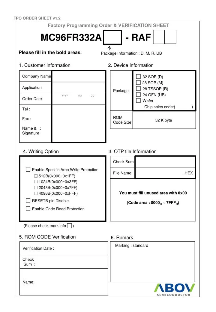
FPO ORDER SHEET v1.2. Factory Programming Order & VERIFICATION SHEET. MC96FR332A - RAF. Please fill in the bold areas. Package Information : D, M, R, UB. 1. Customer Information. 2. Device Information. Company Name. Package. â–¡ 32 SOP (D) â–¡ 28 SOP (M) â–¡ 28 TSSOP (R)

E N D
FPO ORDER SHEET v1.2 Factory Programming Order & VERIFICATION SHEET MC96FR332A - RAF Please fill in the bold areas. Package Information : D, M, R, UB 1. Customer Information 2. Device Information Company Name Package □32 SOP (D) □28 SOP (M) □28 TSSOP (R) □24 QFN (UB) □Wafer Chip sales code:( ) Application Order Date YYYY MM DD Tel : Fax : Name & : Signature ROMCode Size 32 K byte 4. Writing Option 3. OTP file Information □ Enable Specific Area Write Protection □ 512B(0x000~0x1FF) □ 1024B(0x000~0x3FF) □ 2048B(0x000~0x7FF) □ 4096B(0x000~0xFFF) □RESETB pin Disable □ Enable Code Read Protection Check Sum File Name .HEX You must fill unused area with 0x00 (Code area : 0000H ~ 7FFFH) (Please check mark info ) 5. ROM CODE Verification 6. Remark Verification Date : Marking : standard Check Sum : Name:
FPO ORDER SHEET v1.2 Factory Programming Order & VERIFICATION SHEET MC96FR332B - RAF Please fill in the bold areas. Package Information : D, M, R, UB 1. Customer Information 2. Device Information Company Name Package □32 SOP (D) □28 SOP (M) □28 TSSOP (R) □24 QFN (UB) □Wafer Chip sales code:( ) Application Order Date YYYY MM DD Tel : Fax : Name & : Signature ROMCode Size 32 K byte 4. Writing Option 3. OTP file Information □ Enable Specific Area Write Protection □ 512B(0x000~0x1FF) □ 1024B(0x000~0x3FF) □ 2048B(0x000~0x7FF) □ 4096B(0x000~0xFFF) □RESETB pin Disable □ Enable Code Read Protection Check Sum File Name .HEX You must fill unused area with 0x00 (Code area : 0000H ~ 7FFFH) (Please check mark info ) 5. ROM CODE Verification 6. Remark Verification Date : Marking : standard Check Sum : Name: