Download
1 / 13
130 likes | 384 Views
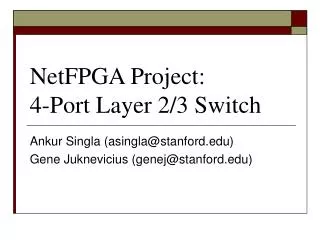
NetFPGA L2 Switch. Sheng-Liang Song ssl@cisco.com EE384Y, Spring 2003. Overview of the NetFPGA Board. SRAM. SRAM. L2Sw4 User FPGA #1. Control FPGA. Ethernet Controller. Port 0. Port 1. Port 2. Port 3. User FPGA #2. Port 4. Port 5. Port 6. SRAM. Port 7.

E N D
NetFPGAL2 Switch Sheng-Liang Song ssl@cisco.com EE384Y, Spring 2003
Overview of the NetFPGA Board SRAM SRAM L2Sw4 User FPGA #1 Control FPGA Ethernet Controller Port 0 Port 1 Port 2 Port 3 User FPGA #2 Port 4 Port 5 Port 6 SRAM Port 7
Overview of the UFPGA (L2 Switch) MemCtrl 4-Port Layer 2 Switch Control RX data RX data TX data TX data CFPGA Interface To/From SRAM Mem DiagCtrl do_mem_diag Request To/From CFPGA Grant mem_diag_done do_mem_diag LEDs[3 : 0] LEDs[3 : 0] LEDs[3 : 0] Button Input
S4-CM FSM Diagram ~mem_diag_done Reset rx_done mem_diag do_ctrl 1.myCtrlFifoNotEmpty mem_diag_done do_mem_diag & ~mem_diag_done ctrl_done ~tx_done ~rx_done try_read tx_done 2.RxEn && |(QRxVector & rxFifoNotEmpty) idle wait_tx_done 3.TxEn rx_done “else” ~Qempty &(|QtxVector & txFifoNotFull) “1” TxEn try_write nxt_rd_port ~TxEn “else” wait
S4-MEM Diag FSM Diagram else Reset idle do_mem_diag & ~mem_diag_done Addr >= Max_addr fill compare Addr >= Max_addr Addr<Max_addr Addr < Max_addr
Registers DeviceID[0xE384] Ver: 0x01 UFPGA_ID[1] Version[7:0] 10: MemDiag Ctrl: 0x02 Ctrl 20: fail Addr:[17:0] Addr: 0x05 [20:18] Phase 31: done Data1:[19:16] = Mem[35:32] Data1: 0x06 Pattern[7:0] Data2:[31:0] = Mem[31:0] Data2: 0x07
S4-MEM FSM Diagram: CFPGA Interface Write Read wait_i_not_empty read_wait0 i_not_empty of_rd_pkt “1” if_wr_pkt Reset write_0 read_wait1 idle ~of_full & ~tx_eop i_not_empty “1” “1” “1” ~of_full&tx_eop write_1 read_wait_not_full write_data_eop write_done of_wr_en Read Write SRAM Addr[que:2][pkt:7][wd:9]
S4-RX_CTRL FSM Diagram: Try_Rd grant_ci_ufpga Getwd0 load_DA0123 rd_rdy_ci_ufpga_d1 deny_ci_ufpga Reset do_ctrl Getwd1 load_DA45SA01 idle rd_rdy_ci_ufpga_d1 ~do_ctrl “1” Getwd2 load_SA2345 WtEOP rd_rdy_ci_ufpga_d1 “1” Getwd3 DoOp load_OpcodeAddr eop_ci_ufpga rd_rdy_ci_ufpga_d1 Getwd4 rd_rdy_ci_ufpga_d1 load_WrData
S4-TX_CTRL FSM Diagram: ~do_tx_ctrl Reset idle do_tx_ctrl Request “1” deny_ci_ufpga “1” done Wt_Grant SendPkt grant_ci_ufpga wr_rdy_ci_ufpga_d1 & tx_ctrl_last word ~(grant_ci_ufpga | deny_ci_ufpga) else
S4-RX FSM Diagram: Try_Rd grant_ci_ufpga Granted do_read rd_rdy_ci_ufpga_d1 ~do_read Reset deny_ci_ufpga idle getDAhi rd_rdy_ci_ufpga_d1 Wt_DAvldl “1” “1” Chk_Match Rx_Done else “1” rd_rdy_ci_ufpga_d1 & eop_ci_ufpga Wt_EOP
S4-TX FSM Diagram: do_write Start_Tx Reset idle “1” deny_ci_ufpga else Wt_Grant “1” grant_ci_ufpga else Granted Done else wr_rdy_ci_ufpga_d1 tx_eop Wt_EOP
References: [1] N. McKeown, “NetFPGA Project.” Online http://klamath.stanford.edu/NetFPGA/, Apr, 2003 [2] S. Gaggara, “Control of the NetFPGA board.” Online http://klamath.stanford.edu/NetFPGA/docs/Control_NetFPGA.pdf [3] Henry Fu, and Harn Hua Ng, “NetFPGA: Documentation for Developing User Modules” Online http://klamath.stanford.edu/NetFPGA/docs/user_doc.pdf [4] “The Sw4 UFPGA.” http://klamath.stanford.edu/NetFPGA/docs/Sw4.pdf [5] Henry Fu, and Harn Hua Ng, “NetFPGA: Design Architecture and Implementation.” Online http://klamath.stanford.edu/NetFPGA/docs/dev_doc.pdf [6] Altera Corporation, "Altera(R) APEX 20K Programmable Logic Devices." Online http://www.altera.com/literature/ds/apex.pdf