Download
1 / 21
210 likes | 550 Views
Abstract : 3-D integrated circuits utilize z-axis allowing unique fabrications designs. This utilization allows cheaper, more compact, and efficient integrated circuits. 3-D IC Fabrication and Devices. Thong Moua Monday April 11 th 2016. Outline. Background information

E N D
Abstract: • 3-D integrated circuits utilize z-axis allowing unique fabrications designs. This utilization allows cheaper, more compact, and efficient integrated circuits. 3-D IC Fabrication and Devices Thong Moua Monday April 11th 2016
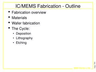
Outline • Background information • Introduction to 3D IC • Fabrication • Benefits/issues • Current technology • Applications
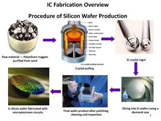
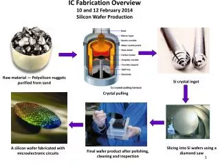
Background info • How integrated circuits are made • Silicon ingot is grown • Sliced into wafers • Chip design is etched on • Wafer is diced according to chip
Introduction to 3-D IC’s • A Single Circuit with two or more layers of active components connected by TVS • Utilizes the z-directional axis to improve performance, reduce power, etc.
Four main types of Fabrication • Monolithic • Wafer-on-Wafer • Die-On-Wafer • Die-On-Die
Fabrication (Wafer-on-Wafer) • Components are built on two or more wafers • Wafers are aligned accordingly • Bonding of the two wafers • Thinning of wafers (can be done before or after bonding) • Wafer is diced
Benefits of 3D IC • Lower fabrication cost • Save space • Allows for miniaturization • Improved performance • Better bandwidth • Reduced power
Issues with 3D IC • Yield • Heat • Design complexity • Testing • Lack of standards
SIP (system in packaging) SiPis multiple bare dice and/or chips mounted on a common substrate, which is used to connect them all together. Packaged together.
2.5D integrated Circuits Package-on-Package (PoP)
Applications • True 3d IC is still in need of further research and development. • Monolithic IC 3D inc. • 3D Logic • 3D memory • 3D electro optics • DRAM (Intel and micron hybrid memory cube)
Conclusion 3-D integrated circuits is the next step in increasing performance of our technology. Its unique design in the z-axis allows for profound benefits, but at a cost of heat, complexity, etc. However further research and development can minimize the cons and allow a more commercialized product.
References • http://www.extremetech.com/computing/197720-beyond-ddr4-understand-the-differences-between-wide-io-hbm-and-hybrid-memory-cube • http://www.monolithic3d.com • http://www.invensas.com/Company/Documents/Invensas_IPCAPEX2013_3D.pdf • http://www.eetimes.com/document.asp?doc_id=1279540 • http://www.xilinx.com/programmable/about/research-labs/3-D_Architectures.pdf • https://en.wikipedia.org/wiki/Three-dimensional_integrated_circuit • All Images provided by Google
5 key concepts • 3D IC is a integrated circuit by stacking wafers/dies so they behave as one single device. • Four main types of fabrication; Monolithic, Wafer-on-Wafer, Die-on-Wafer, Die-on-Die • Benefits of 3D IC • Issues of 3D IC • Applications; HMC and Vertex-7 2000t