Download
1 / 60
600 likes | 737 Views
Student Lecture Fall 2011 ME 4447/6405 Introduction to Mechatronics Georgia Institute of Technology Date: Nov 22, 2011. DAC, Diodes and TRIACS. Paragkumar Thadesar James “Ryan” Cole Prithiviraj Jothikumar Mike Weiler. Outline:. Paragkumar : What is digital to analog converter (DAC)?

E N D
Student Lecture Fall 2011 ME 4447/6405 Introduction to Mechatronics Georgia Institute of Technology Date: Nov 22, 2011 DAC, Diodes and TRIACS ParagkumarThadesar James “Ryan” Cole PrithivirajJothikumar Mike Weiler
Outline: • Paragkumar:What is digital to analog converter (DAC)? • Paragkumar:Types of DAC • Binary Weighted Resistor • R-2R Ladder • Ryan: Discuss Specifications: • Reference Voltages • Resolution • Speed • Settling Time • Linearity • Errors • Ryan:Applications • Prithviraj:Diodes: Theory and applications • Ideal vs. real • Types: Junction and Zener • Mike:Triacs: Theory and applications
What is Digital-to-Analog Converter (DAC) ? • DAC is a device that converts digital numbers (binary) into an analog voltage or current output. 1001 0101 0011 0111 1001 1010 1011 DAC
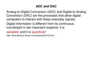
DAC V/s ADC • ADCs are used in systems to capture “real world” signals and convert them to “digital” signals. • DACs are used in systems to capture “digital” signals and convert them to “real world” signals that humans can interpret.
Significance of Reference Voltage in DACs • DACs use input reference voltage to generate analog output from digital signals. DAC DAC (using Vref and bits as input) inside an SAR ADC As explained in earlier student lecture on ADC
Analog Levels For Sampled Digital Values • Each binary number sampled by a DAC corresponds to a different output analog level between “0and Vref” for Unipolarand “Vref and –Vref” for Bipolar.
3 Stages in a DAC • There are 3 stages in a DAC: 1. Binary to level conversion 2. Zero-order hold 3. Recovery filter Binary to Level Conversion Zero-Order Hold Recovery Filter V(n) V(t) Digital-to-Analog Converter (DAC)
Reconstruction of Sine Wave by Bipolar DAC Staircase signal generated using “latch circuits” to latch a particular level after sampling until next level is sampled Analog signal generated after removing harmonics from staircase signal using “low pass recovery filter” Levels gerenated by sampling groups of binary data Group of binary data (E.g. Group of 4 bits) Binary to Level Conversion Zero-Order Hold Recovery Filter V(n) V(t) Digital-to-Analog Converter (DAC)
Types of DAC Implementations • There can be several types of DAC implementations. Some of them are: 1. Binary-weighted resistor 2. R-2R ladder 3. Pulse-width modulation 4. Oversampling DAC (in EVB used in lab) 5. Thermometer-coded DAC 6. Hybrid DAC Covered in this presentation
1. Binary-weighted resistor DAC Concept #1 from past lecture • Inverting summer consists of 3 parts: 1. An inverting Op-Amp 2. Input voltages either high or ground 3. Adjustment of resistor weights to obtain desired output.
1. Binary-weighted resistor DAC Concept #2 from past lecture Gain of Inverting Op-Amp • Vout = -Vin * (Rf /Rfin) = - I * Rf
1. Binary-weighted resistor DAC • Details • Assumptions: • Virtual Ground at Inverting Input • Vout = -IRf • Use Vref as input voltage • Use transistors to switch between high and ground • Use resistors scaled by two to divide voltage on each branch by a power of two • V1 is MSB, V4 LSB in this circuit
1. Binary-weighted resistor DAC • Example: take a 4-bit converter, • Rf /R= a; a = gain. • Here ‘a’ should not be ~1000 as in strain gage lab because here inputs for DAC are Vref and they are in terms of volts where as in strain gage lab input was in terms of millivolts for ADC. • Input parameters: • Input voltage Vref = -2V • Binary input = 1011 • Coefficient a = ½
1. Binary-weighted resistor DAC • Resolution: Making LSB as 1 and all other inputs as 0, • If Rf = R/2 then resolution is • Max Voutcan be obtained making all input bits equal to 1 and it can be obtained solving geometric series in equation (1) as
1. Binary-weighted resistor DAC • Advantages: • Simple • Fast • Disadvantages • Need large range of resistor values (2048:1 for 12-bit) with high precision in low resistor values. • Need very small switch resistances.
2. R-2R Ladder DAC B2 B1 Ladder of 2 Resistor Values R and 2R at Input of Inverting Op-Amp B0 • All the inputs are Vref followed by switches. Output of switches is B2, B1 and B0 in above circuit. • Similar to binary weighted DAC, status of switches would define if input bits to DAC are Vref or 0.
2. R-2R Ladder DAC B2 B1 Ladder of 2 Resistor Values R and 2R at Input of Inverting Op-Amp B0 • Circuit may be analyzed using Thevenin’s theorem (replace network with equivalent voltage source and resistance). • Final result is: 2
2. R-2R Ladder DAC • Resolution: Making LSB as 1 and all other inputs as 0, • If Rf = R then resolution is • Max Voutcan be obtained making all input bits equal to 1 and it can be obtained solving geometric series in equation (1) as
2. R-2R Ladder DAC • Advantages: • Only 2 resistor values • Lower precision resistors acceptable • Disadvantages • Slower conversion rate
Outline: • Paragkumar:What is digital to analog converter (DAC)? • Paragkumar:Types of DAC • Binary Weighted Resistor • R-2R Ladder • Ryan: Discuss Specifications: • Reference Voltages • Resolution • Speed • Settling Time • Linearity • Errors • Ryan:Applications • Prithviraj:Diodes: Theory and applications • Ideal vs. real • Types: Junction and Zener • Mike:Triacs: Theory and applications
Reference Voltage ( • The reference voltage determines the range of outputs from the DAC • For Non-Multiplying DAC • Vref is internally set by the manufacturer and is a constant value • For Multiplying DAC • Vref is externally set and can be varied during operation
Full Scale Voltage and Resolution • Full Scale Voltage (Vfs) is the output voltage when all bits are set high • The DAC resolution is the change in voltage due to an increment by the least significant bit (LSB) • Data sheets list the resolution in bits • Typical resolution is 8 – 16 bits N = # of Bits *Resolution depends on ratio of Rf and R as explained in previous section. This case is similar to R-2R ladder resolution with Rf=R
Sampling Rate ( • The sampling rate is the rate at which the DAC can convert the digital input into an output voltage • The Nyquist Criterion is used to ensure the output correctly represents the digital input • fmax is the max frequency of the analog signal to be reconstructed • fs is limited by the input signal clock speed and DAC settling time
Settling Time • The settling time is the interval between a command to update (change) its output value and the instant it is within a specified percentage of its final value • DAC Limiters • Slew Rate of output amplifier– the maximum rate of change of a signal • Amplifier Overshoot and Ringing
Linearity • The linearity is the relationship between the output voltage and the input signal • Ideally the DAC would produce a linear slope
Errors Common DAC Errors: • Offset Error • Gain Error • Full Scale Error • Resolution Errors • Non Linearity • Non-Monotonic • Settling Time and Overshoot
Offset Error • An offset error will cause all the output voltages to be different from the ideal output by the error • It can be determined by measuring the output voltage for a digital input of zero.
Gain Error • The gain error is how well the slope of the actual transfer function matches the slope of the ideal transfer function • It can be determined by measuring the output voltage for a digital input of all 1’s
Full Scale Error • Full Scale error is the combination of the Gain Error and the Offset Error
Resolution Error • The resolution will determine how close your output will match the desired signal 1 Bit Resolution 3 Bit Resolution
Differential Nonlinearity Error (DNL) • The difference between two successive digital output codes is ideally 1 VLSB • The deviation from a step of 1 VLSB is the DNL error • Manufacturers will specify the maximum DNL error
Integral Linearity Error (INL) • The INL is the difference in the ideal linear voltage and the actual output voltage for a given digital code • Manufactures will specify the max INL error
Non-Monotonic • Monotonic Function • A monotonically increasing function will always increase or remain constant (non-decreasing) • A monotonically decreasing function will always decrease or remain constant (non-increasing) • If an increase in the digital input results in a decrease in the output voltage the DAC is considered non-monotonic • If the DNL error is less than ± 1 LSB the DAC is guaranteed to be monotonic
Applications • Audio/Video • MP3 Players • CD Players • Cellphones • USB Speakers • Analog Monitors • Signal Generators • Sine Wave generation • Square Wave generation • Random Noise generation
Outline: • Paragkumar:What is digital to analog converter (DAC)? • Paragkumar:Types of DAC • Binary Weighted Resistor • R-2R Ladder • Ryan: Discuss Specifications: • Reference Voltages • Resolution • Speed • Settling Time • Linearity • Errors • Ryan:Applications • Prithviraj:Diodes: Theory and applications • Ideal vs. real • Types: Junction and Zener • Mike:Triacs: Theory and applications
Diodes • Brief review of semiconductors • Junction Diodes • Zener Diodes • Other type of Junction Diodes
Review • The conduction band allows the electrons to move within the atomic lattice of the material • The valence bandis an energy region wherethe states are generally filled • Electrons in the valence band can be moved to the conductionband with the applicationof energy, usually thermal energy
Semiconductors • A material can be classified as: 1. Insulator – has valence and conduction bands well separated 2. Semiconductor – has valence band close to conduction band (the energy gap is about 1eV). 3. Conductor – has the conduction and valence bands overlapping • Semiconductors two unusual properties: 1. Conductivity increases exponentially with temperature 2. Conductivity can be increased and precisely controlled by adding small impurities in a process called doping.
Majority carriers p n Depletion Region Diode • A diode is created when a p-type semiconductor is joined with and n-type semiconductor by the addition of thermal energy. • When both materials are joined, the thermal energy causes positive carriers in the p-type material to diffuse into the n-type region and negative carriers in the n-type material to diffuse into the p-type region. • This creates the depletion region within the diode
Depletion Region Original Size p n p n if Reverse Biased Forward Biased Forward and Reverse biased • A diode is forward biased if the positive terminal of the battery is connected to the p-type material. • Current is sustained by the majority carriers. • A diode is reverse biased if the positive terminal of the batteryis connected to the n-type material. • There is a small reverse currentor leakage currentsustained by the minority carriers • If reverse bias is sufficiently increased, a sudden increase in reverse current is observed. This is known as the Zener or Avalanche effect Depletion Region Original Size V V
I conduction region V non-conduction region Ideal Curve Diode Characteristic Curve Ideal Diode – no resistance to current flowin the forward direction and infinite resistancein the reverse direction.
Zener Diode • Zener diodes operate in the breakdown region. • Zener diodes have a specified voltage drop when they are used in reverse bias. • Every p-n junction (i.e. diode) will break down in reverse bias if enough voltage is applied. • Able to maintain a nearly constant voltage under conditions of widely varying current. • Zenerdiodes are operated in reverse bias for normal voltage regulation.
Other Types of Diodes • Light Emitting Diodes (LEDs) - A diode formed from a semiconductor such as gallium arsenide, carriers that cross the junction emit photons when they recombine with the majority carrier on the other side. • Photodiode – Exploits the fact that all semiconductors are subject to charged carrier generation when they are exposed to light. Photodiodes are often used to sense light such as in an Opto-isolator.
Outline: • Paragkumar:What is digital to analog converter (DAC)? • Paragkumar:Types of DAC • Binary Weighted Resistor • R-2R Ladder • Ryan: Discuss Specifications: • Reference Voltages • Resolution • Speed • Settling Time • Linearity • Errors • Ryan:Applications • Prithviraj:Diodes: Theory and applications • Ideal vs. real • Types: Junction and Zener • Mike:Triacs: Theory and applications
Dr. Ume What are TRIACS? Dr. Ume, what are TRIACS?
What are TRIACS? • Triode for Alternating Current • Electronic component that can conduct current in either direction (bidirectional) when triggered • Bidirectionality makes TRIACs excellent switches for AC currents -> can handle large power flows • Used in high power switching applications i.e. hundreds of amps / thousands of watts
How do TRIACs work? • To understand operation of TRIACs, we first need to explain Thyristors… How do TRIACs work?
What are Thyristors? • Class of semiconductor components that can only go in 1 direction. • Wide range of devices, SCR (silicon controlled rectifier), SCS (silicon controlled switch), Diacs, Triacs, and Shockley diodes • Used in high power switching applications • i.e. hundreds of amps / thousands of watts
How do Thyristors work? • Unidirectional semiconductor • PNPN (4-layer) device: • PNP and NPN transistor back-to-back. • With forward voltage, small gate current pulse turns on device. • Once on, each transistor supplies gate current for the other, so no need for gate input