Download
1 / 11
110 likes | 312 Views
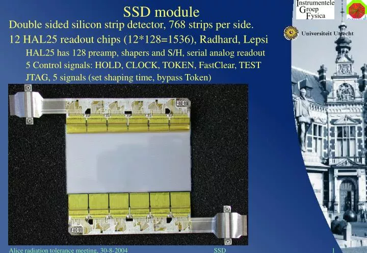
SSD module. Double sided silicon strip detector, 768 strips per side. 12 HAL25 readout chips (12*128=1536), Radhard, Lepsi HAL25 has 128 preamp, shapers and S/H, serial analog readout 5 Control signals: HOLD, CLOCK, TOKEN, FastClear, TEST JTAG, 5 signals (set shaping time, bypass Token).

E N D
SSD module Double sided silicon strip detector, 768 strips per side. 12 HAL25 readout chips (12*128=1536), Radhard, Lepsi HAL25 has 128 preamp, shapers and S/H, serial analog readout 5 Control signals: HOLD, CLOCK, TOKEN, FastClear, TEST JTAG, 5 signals (set shaping time, bypass Token) SSD
ALICE SSD sub-detector ALICE SSD sub-detector contains 1698 SSD-modules Layer 5: 34 ladders, 22 SSD-mod. per ladder Layer 6: 38 ladders, 25 SSD-mod. per ladder 2 ECM per ladder ECM connected with 10..13 SSD-mod. ECM mediates power and signals: • 10..13 analog signals • 5 LVDS control signals • 5 LVDS JTAG signals • 1 LVDS error signal ECM developed at NIKHEF Per Side 72 ECMs, total 144 ECMs ECM Alcapone & Alabuf chips are made in IBM .25 radtolerant technology ECM COTS regulator power transistor tested for radiation SSD
SSD ELECTRONICS LOCATION: PASSERELLE A-SIDE RACKS A14, A15, A28, A29 A14 AND A29: FEROM READOUT SYSTEM EIGHT 6U VME CRATES A15 AND A28: CAEN SY1527 POWERSUPPLY SYSTEM SIX 8U SY1527 CRATES FEROM SYSTEM CONTAINS ADC SYSTEM FOR READOUT OF SILICON STRIP MODULES, INTERFACE TO DAQ, TRIGGER AND SLOW CONTROL SSD
L1/L2 TTC FEROM system SSD sub-detector CTP L0 (lvds) 10...13 x Analog ECM 1 SSD-module 1 Busy (lvds) control (5xlvds) … error (1xlvds) DAQ JTAG (5xlvds) DDL fiber SSD-module 10…13 ECM 2 DCS JTAG Slow control CAN ECM 144 FEROM system interface FEROM system communicates with: • 144 ECMs (1698 analog output signals) • CTP (Central Trigger Processor) • L0&Busy via LVDS • L1/L2 TTC system • DAQ (DDL) • DCS (JTAG) • Slow Control (CAN) CTP>Take 1536 samples from each ECM analog output>DAQ SSD
L1/L2 TTC FEROM system SSD sub-detector CTP L0 (lvds) 10...13 x Analog ECM 1 SSD-module 1 Busy (lvds) control (5xlvds) … error (1xlvds) DAQ JTAG (5xlvds) DDL fiber SSD-module 10…13 ECM 2 DCS JTAG Slow control CAN ECM 144 CAN CAN FEROM Crate 4 FEROM Crate 8 FEROM Crate 1 power supply FEROM Crate 5 power supply V430 backplane 10sl V430 backplane 10sl V430 backplane 10sl V430 backplane 10sl LINKm ADm1 ADm2 .. ADm9 LINKm ADm1 ADm2 .. ADm9 LINKm ADm1 ADm2 .. ADm9 LINKm ADm1 ADm2 .. ADm9 L0 L0 JTAG L0 L0 JTAG Busy Busy Busy Busy L0 L0 BUFMUX1 BUFMUX2 Busy Busy FEROM ADm 9 ECM 9 L1/L2 TTC LINK- module CTP ADm 2 ECM 2 ADm 1 ECM 1 12 x Analog diff L0 Busy FEROM BUS (V430) control (5xlvds) L0 (lvds) BUF MUX Busy (lvds) JTAG (5xlvds) DDL fiber DAQ error (1xlvds) JTAG DCS SSD
ADC 0…5 BUS-FPGA FEROM BUS AD-FPGA1 ADC Offset ZSU ADC Offset ZSU FIFO BUFFER ADC Offset ZSU ADC Offset ZSU MEB 1 SRAM 64Kx32 ADC Offset ZSU ADC Offset ZSU ADC 6…11 AD-FPGA 2 Offset+ZSU SRAM 16Kx32 ADC Offset ZSU ADC Offset ZSU BUFFER ADC Offset ZSU ADC Offset ZSU MEB 2 SRAM 64Kx32 ADC Offset ZSU ADC Offset ZSU AD-module architecture 200 AD-modules => Effort to reduce cost price 12 inputs, functionality simple, low cost FPGAs 12 bit ADC & digital offset correction, increase dynamic range MEB reduces dead time to 150 µs (SEB 400 µs @ 5% occupancy) SSD
FEROM BUS Standard VME64 too slow, and no 3,3V available Dedicated synchronous VME backplane protocol above cPCI Lower cost price More flexible, 3,3V & 1,8V, Sending double words Easier to couple with the DDL, DDL-like protocol FEROM crate backplane split up in 2 x 10 slots Reducing scope single point failures Doubles data bandwidth due to doubling number of DDLs (30 MHz) Crates produced by Wiener, ordered via CERN ESS group Good supply and availability Using standard CAN control for crate power supplies and fans Slot number: provides address Adm (data bus & JTAG switch) AD-modules use standard combinatoric TTL comparators. (reduce SEU) SSD
Link module • Most link-module functionality implemented in 1 FPGA • DDL (SIU-piggyback) • CTP (LVDS L0/BUSY, TTCrq piggy back) • FEROM-bus • Many signals (300 I/Os) => FPGA in BGA package • Advantages FPGA implementation: • FPGA introduces lot of flexibility. • Link Module SEB implemented with FPGA DPM • Xilinx VirtexII redundancy in input configuration.bits (reduce SEU) • Link Module accommodates FPGA configuration PROMs. • For AD-module and link-module FPGAs • Radhard PROM optional • Link module provides JTAG interface for DCS SSD
Radiation at FEROM location SSD Rack locations K+L+M radiation calculations (passerelle A-side rack loc. A14,15,28,29) 10 year running period Our racks are located halfway between pos. K and L and halfway between pos. L and M Assumed 1MeV n-equ. fluence (ref. Table 9) : 1. 10E8/cm2 Hadron >20MeV fluence factor 10 lower: 1. 10E7/cm2 Assumed running time: 10E7 sec. So flux hadron >20MeV flux 1/cm2.sec. SSD
FEROM SEU calculation Assumed SEU cross section for FPGA and SRAM memories 10-13 cm2/bit. (For the SRAM’s, this seems a fairly good estimate, for the FPGA’s no real data at this moment available). Also for the configuration PROM no real data available. Error rate using assumed cross section: 10-13/bit.sec 10 % of FPGA’s total config memory: 34 Mega-bits • Error rate: 34E6x10-13= 3.4 10E-6 bits/sec. Aprox. 1 bit/ 80hrs • SEU can hang-up system. • Ferom has JTAG which allows partial readback and reconfiguration Offset and zero suppress memory: 40 Mega-bits • Error rate: 40E6x10-13 = 4E-6 bits/sec. Aprox. 1 bit/70 hrs. • No system hang-up, SEU detected by readback after every run Event data memory: 14 Mega-bits (5% occupancy, All 4MEB in use) • Error rate: 14E6x10-13 = 14E-7 bits/sec. Aprox. 1 bit/200 hrs. • No system hang-up, SEU detected with a parity mechanism FEROM crates are standard LHC VME crates with controller and memories as well! No data available? SSD
SSD POWER SUPPLY SYSTEM MODULARITY: 144 HALF LADDERS WITH DOUBLE SIDED SLICON STRIP DETECTORS EACH HALF LADDER USES 3 FLOATING L.V. SUPPLIES AND 1 FLOATING SENSOR BIAS H.V. SUPPLY • P-SIDE: 7V 4A • N-SIDE: 7V 4A • GND. SIDE: 7V 2A • H.V. BIAS: 250V 0,1/1Ma H.V. BIAS IS USED SYMETRICALLY, MIDPOINT GROUNDED POWER SUPPLY SYSTEM: CAEN SY1527 CHOSEN BECAUSE MODULARITY AND AVAILABLE OUTPUTS CORRESPOND VERY WELL TO OUR NEEDS: L.V. MODULES HAVE 2 GROUPS OF 3 FLOATING OUTPUTS, ETC. BOTH CAEN EASY SYSTEM AND WIENER ARE NOT SUITABLE WITHOUT (PARTIAL) REDESIGN : NON-FLOATING OUTPUTS AND COMPLETELY DIFFERENT MODULARITY SSD