Download
1 / 21
220 likes | 561 Views
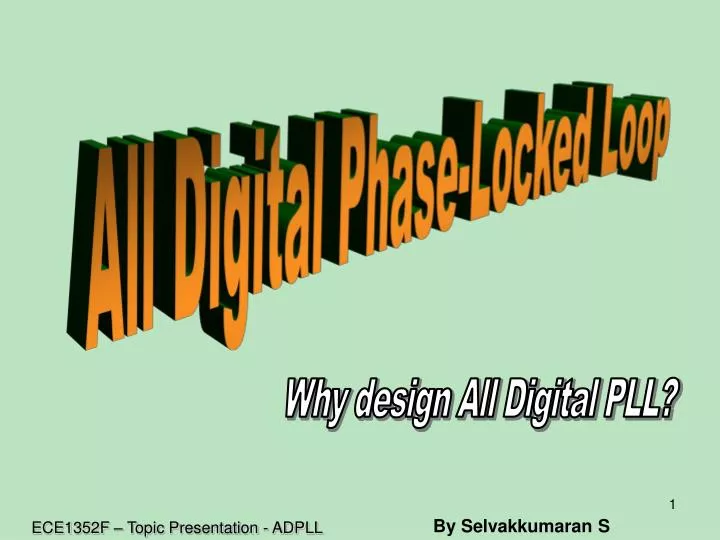
All Digital Phase-Locked Loop. Why design All Digital PLL?. By Selvakkumaran S. ECE1352F – Topic Presentation - ADPLL. Up. D Q CK. A. B. CK D Q. Dn. What is an All Digital Phase-Locked Loop (ADPLL)?. Some Analog PLLs have utilized pure digital components before

E N D
All Digital Phase-Locked Loop Why design All Digital PLL? By Selvakkumaran S ECE1352F – Topic Presentation - ADPLL
Up D Q CK A B CK D Q Dn What is an All Digital Phase-Locked Loop (ADPLL)? • Some Analog PLLs have utilized pure digital components before e.g: Charge-pump PLLs utilized Phase Frequency Detector consisting of 3-state finite state machine with two flip-flops ECE1352F – Topic Presentation - ADPLL
Digital Phase Detector Digital Loop Filter fout fin Digital VCO What is an ADPLL? (contd.) • All Digital PLLs consist only of digital components • The first All Digital PLL was reported by Drogni [1967] ECE1352F – Topic Presentation - ADPLL
Why All Digital PLL? Improvements in digital designs *Progress in increasing *Progress in reducing • Performance • Size • Speed • Cost • Reliability * Portability/ Reusability * Programmability * Testability ECE1352F – Topic Presentation - ADPLL
Why All Digital PLL? Solves Problems Related to Analog PLLs(APLL) • Sensitivity to DC Drifts • Component Saturations • Difficulties building higher order loops • Initial calibration and periodic adjustments ECE1352F – Topic Presentation - ADPLL
Issues of ADPLLs versus APLLs • Limitation on operating speed • Chip area • Power Consumption • Worse jitter performance due to D/A converter resolution limitation * Note: The above issues need further exploration[7] as some papers have reported better ADPLL performance. ECE1352F – Topic Presentation - ADPLL
Example ADPLL Loop Filter • Up/Down control from the Phase Detector Controls the Counter value or the Digital Phase difference – Transfer Function ~ 1/sTi Up/Down Counter ECE1352F – Topic Presentation - ADPLL
Example Digital VCO (DCO) • Up/Down Counter Value or the Phase Error is utilized to create the clock %N Counter ECE1352F – Topic Presentation - ADPLL
ADPLL Design Analysis Z-transform technique[5,6] • z domain transfer function • Solutions within the unit circle ensures stability ECE1352F – Topic Presentation - ADPLL
ADPLL Design Example 1[2] ECE1352F – Topic Presentation - ADPLL
Results [2] 3.3V Supply
Results[2] • Shorter Locking in time • Better Jitter Performance • Better Portability (cell-based design) • Reduced circuit complexity • Reduced Design Time • Note: Some other papers have reported ADPLLs area and power statistics better than APLLs ECE1352F – Topic Presentation - ADPLL
ADPLL Design Example 2[6] A Second order ADPLL C2(Z-1)+C1 2hwnS + wn2 H(z)= H(S)= (Z-1)2+C2(Z-1)+C1 S2 + 2hwnS + wn2 ECE1352F – Topic Presentation - ADPLL
Acquisition Behaviour[6] *ADPLL shows a better performance in terms of the acquisition time ECE1352F – Topic Presentation - ADPLL
Phase JitterBehaviour[6] ECE1352F – Topic Presentation - ADPLL
Results[6] • Larger lock-in range (~4.5 x APLL) • Larger Hold-in Range than APLL • Smaller RMS Phase Jitter • Digital approach to design • Software configurability/ programmability ECE1352F – Topic Presentation - ADPLL
Summary - Why are ADPLLs better? • Stability • Fast Acquisition Time • Large hold-in range • Large lock-in range • Better phase jitter performance • No need for off-chip components • Technology portability • Testability • Programmability • Simpler design and faster simulation ECE1352F – Topic Presentation - ADPLL
Future of ADPLL • Digital IP (Intellectual Property) vendors are already creating ADPLL products • As technology progress happens skew problems will require ADPLLs within the design components to synchronize the clock signal between various blocks ECE1352F – Topic Presentation - ADPLL
References • Behzad Razavi, Design of Analog CMOS Integrated Circuits, McGraw-Hill, 2001 • Ching-Che Chung and Chen-Yi Lee, “An All-Digital Phase-Locked Loop for High Speed Clock Generation, IEEE J. Solid-State Circuits, vol 38, No.2, pp347-351, February 2003 • Thomas Olsson and Peter Nilsson, “A Digitally Controlled PLL Using a Standard Cell Library”, Lund University, Sweden, www.es.lth.se/home/ton • Roland E. Best, Phase-Locked Loops, Design, Simulation and Applications, 4th Ed, McGraw-Hill, 1999 (Chapter 4, pp177-228) • Venceslav F, Kroupa, Phase Lock Loops and Frequency Synthesis, Wiley, 2003, (Chapter 10, pp231-254) ECE1352F – Topic Presentation - ADPLL
References (contd.) • Y.R.Shayan, T.Le-Ngoc, “All Digital phase-locked loop: concepts, design and applications”, IEE Procedings, Vol.136, Pt. F. No.1, pp53-56, February 1989 • Dao-Long Chen, “A Power and Area Efficient CMOS Clock/Data Recovery Circuit for High-Speed Serial Interfaces, IEEE J. of Solid-state Circuits, Vol. 31, No8, pp1170-1176, August 1996 ECE1352F – Topic Presentation - ADPLL