Download
1 / 15
310 likes | 717 Views
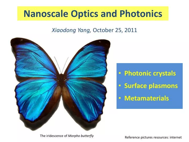
Nanoscale Optics and Photonics. Photonic crystals Surface plasmons Metamaterials. Xiaodong Yang, October 25, 2011. The iridescence of Morpho butterfly. Reference pictures resources: internet. The scale of things. The electromagnetic spectrum. Electronics and photonics roadmaps.

E N D
Nanoscale Optics and Photonics • Photonic crystals • Surface plasmons • Metamaterials Xiaodong Yang, October 25, 2011 The iridescence of Morphobutterfly Reference pictures resources: internet
Electronics and photonics roadmaps Electronic integrated circuits Transistor Vacuum tube Fast, low-cost, scalable and functional integrated devices Early electronics Nanofabrication and nanomanufacturing techniques Nanophotonic integrated circuits Optical MEMS Geometrical optics
Photonic crystals in nature Peacock feather Morpho butterfly Sea Mouse hair Natural opals λ/2
Photonic crystals and defects Photonic crystal: periodically structured electromagnetic media, generally possessing photonic band gaps. Lattice constants are comparable to the wavelength of light in the material. Point defect: cavity Line defect: waveguide λ/2
Surface Plasmons Gothic stained glass rose window of Notre-Dame de Paris
εd Evanescent field εm |Ez| λSP<<λ0 Surface Plasmons at metal-dielectric interface • Strong light localization near the • metal-dielectric interface • Surface Plasmons with large k • SP wave interference 10 µm
l λ a a Metamaterials: beyond natural materials Natural materials “atoms” • Atomic lattice constant a ~ 5.65 Å • Optical wavelength λ ~1μm • Homogeneous medium Crystal structure of sodium chloride (NaCl) Metamaterials “meta-atoms” • Artificially fabricated structures • Unit cell a << wavelength λ • Effective-media theory can be applied • Material properties not existing in natural materials
Negative Index of Refraction n ε < 0,µ < 0 = n < 0
Negative Index of Refraction Snell’s Law
Photonic integrated circuits • Photonic crystals • Surface plasmons • Metamaterials
Optical communications Consumer electronics Industrial applications • Photonic crystal fibers • Photodetectors • Optical switches • Semiconductor lasers • CCD imaging • LCD and LED displays • Photolithography • Laser manufacturing • High-power fiber lasers Renewable energy Biomedical • Solar energy harvesting • Thin-film photovoltaics • LED lighting • Biosensors • Fluorescence imaging • Cancer therapy • Applications of nanoscale optics and photonics Nanoscale Optics and Photonics