Download

1 / 16
160 likes | 242 Views
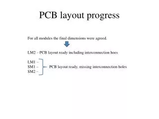
Proposal for NSW chamber PCB layout and alignment (updates). Some remarks about mechanical layout. After the discussions with G. Spigo and M. Ciapetti and checking the sector layout and overlap regions the angles for the MM modules defined: LM1 – 33° LM2 – 8 ° SM1 & SM2– 21°

E N D
Proposal forNSW chamber PCB layoutand alignment(updates) Givi Sekhniaidze
Some remarks about mechanical layout • After the discussions with G. Spigo and M. Ciapetti and checking the sector layout and overlap regions the angles for the MM modules defined: • LM1 – 33° • LM2 – 8° • SM1 & SM2– 21° • Small and large sectors will have the different pitches for the strips (450 μm for LM and 425 μm for SM) • The PCBs will NOT have the equal height: • For intermediate PCBs (PCB2,3,4 for LM/SM1 and PCB7 for LM/SM2) it will be calculated as 1024 x Pitch (460.8mm for LM and 435.2mm for SM) • The rest of the module height will be equally distributed between external PCBs • The height of the external PCBs will be slightly larger then intermediate (example: 474.4mm vs. 460.8mm for LM2), but due to the spacer/mesh frame (25mm minimum) the active area will be less. Givi Sekhniaidze
Overlap Givi Sekhniaidze
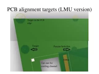
Proposal for PCB alignment (MSW version) • We propose to have one pair of the precise hole and slot in the centralpart of the PCB • Precise hole will be used ONLY once during positioning on the gluingtable • In the frame of the panel could be glued precise insert (Inox, PEEK, etc.) for alignmentwith other panels Assembling holes Precise slot Precise hole D Assembling holes Givi Sekhniaidze
Proposal for multi-PCB alignment 3 board version Precise holes in the table Panel assemblingtable Givi Sekhniaidze
PCB in-plane alignment Additional Targets/images Precise hole MSW version Read-out strips Strip 513 Strip 512 MMFE-8 Givi Sekhniaidze
Alignment check of PCBs on readout panels Measurements taken with a laser machine from NA62 lab (CERN-PH-DT)
Scan direction Scan performed on both sides of the readout eta panel with the precise pin inserted in the same hole on the two sides Alignment pin Srripsroted to the PCB edge • Readout Eta
Strips far from the pin δ < 20 μm • Strips close to the pin δ ≈ 35 μm
Assembling holes for LM2 chamber • As an example, part of the PCB6 from LM2 chamber • The assembling holes are equally distributed in the frame area • Only one hole in the center of the connector area Givi Sekhniaidze
MMFE board and spacer/mesh frame • The dimensions of the MMFE board will be 50mm x 215 mm • The space between spacer/mesh frame and edge of the R/O board – 55 mm(50 mm MMFE width + 5 mm clearance) MSW NSW MMFE Givi Sekhniaidze
Assembling holes in connector area • Preferable position for assembling holes w.r.t. connector would be in the center of the connector (free space between two Zebra connectors) Assembling holes R/O strips Zebra connectors Givi Sekhniaidze
Summary • The draft version for the PCB layouts are ready– Missing the routing for the Zebra connectors – need position of the holes– Number and positions of the interconnection holes to be decided a.s.a.p.– Final decision about dimensions and the shape of the spacer/mesh frame (combined or separate) is needed to finalize the PCB design (resistive strips, HV distribution, pillars, etc.) • Alignment method for the PCB positioning – MSW version + Saclay + other ideas? • Other targets/images for in-plane alignment to be implemented in PCB design? • Other wishes, ideas, suggestions? Givi Sekhniaidze