Download
1 / 28
280 likes | 445 Views
Nanometer-scale Organic Molecular Recording with Scanning Tunneling Microscopy. Pennycook, S. J. et al . Phys. Rev. Lett. 2000, 84 , 1780. Gao, H.-J. et al . Appl. Phys. Lett. 2000, 77 , 3203. Liu, Z. F. et al . Adv. Mater. 2005, 17 , 459. Tobe Lab. FUJITA Takumi. Contents.

E N D
Nanometer-scale Organic Molecular Recording with Scanning Tunneling Microscopy Pennycook, S. J. et al. Phys. Rev. Lett. 2000, 84, 1780. Gao, H.-J. et al. Appl. Phys. Lett. 2000, 77, 3203. Liu, Z. F. et al. Adv. Mater. 2005, 17, 459. Tobe Lab. FUJITA Takumi
Contents • Introduction STM Data Storage Organic Charge-Transfer Complex • Writing and Erasing Nanometer-Scale Marks • Thermochemical Hole Burning • Summary
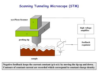
STM Memory (Potential) 0.9 Pb/cm2 ≈ 6 Pb/in2 (Pb; petabits = 1015 bits) Introduction Data Storage Transition of Surface Recording Density of Magnetic Storage (bits/in2) Magnetic Storage …used as HDD in PC ~ 200 Gb/in2 (Gb; gigabits = 109 bits) ●InLaboratory ●Commercial Products
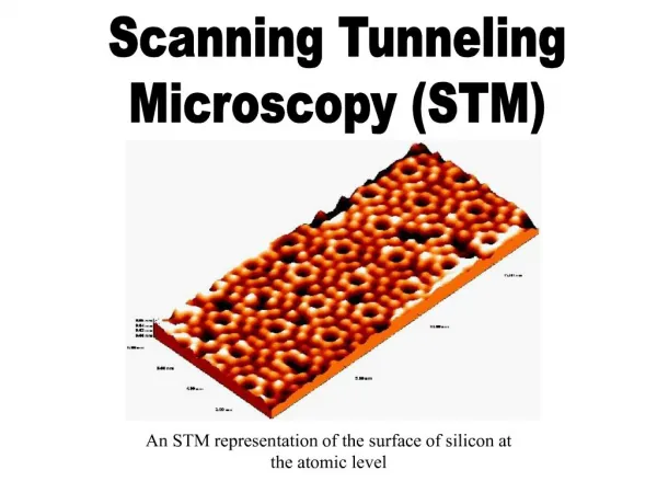
Introduction Scanning Tunneling Microscopy (STM) Tobe Lab. 中国科学院物理研究所 纳米物理与器件实验室
Introduction STM Memory Bright spots indicate relatively higher conductance.
Introduction • Advantages of Organic Materials for Electronic Devices • Lower Cost • Easy Synthesis • Controllable Properties • Requirements for Samples of STM Memory • Uniform Surface in Atomic Scale • Conductivity Organic Charge-Transfer (CT) complex
Introduction CT complex (In most cases) • Composed of… • Electron Donor • Electron Accepter p-Conjugated Backbone + Donor/Accepter Substituent Donor Molecule Donor Substituents Accepter Substituents e- 3~4 Å Accepter Molecule
Reversible, Nanometer-Scale Conductance Transitions in an Organic Complex Gao, H. J.; Sohlberg, K.; Xue, Z. Q.; Chen, H. Y.; Hou, S. M.; Ma, L. P.; Fang, X. W.; Pang, S. J.; Pennycook, S. J. Phys. Rev. Lett.2000,84, 1780-1783. Direct observation of a local structural transition for molecular recording with scanning tunneling microscopy Shi, D. X.; Song, Y. L.; Zhang, H. X.; Jiang, P.; He, S. T.; Xie, S. S.; Pang, S. J.; Gao, H. J. Appl. Phys. Lett.2000,77, 3203-3205.
Sample; CT complex of NBMN-pDA Donor Accepter Polycrystalline Film on HOPG • By Deposition • Thickness of 20 nm • 1:1 Molar ratio of Donor and Accepter Materials pDA (1,4-phenylenediamine) NBMN (3-nitrobenzal malonitrile) Images of film surface STM TEM 6 × 6 nm2 600 × 600 nm2 HOPG; Highly Oriented Pyrolytic Graphite 高配向グラファイト TEM; Transmission Electron Microscope 透過電子顕微鏡
Writing Marks on the Film Writing condition Imaging condition Constant Height Mode Vb = 0.19 V,It = 0.19 nA Voltage Pulses 3.5 ~ 4.2 V, 1 ms Distance of Marks ca. 1.7 nm Still Identified after 2 Weeks
Erasing the Marks Erasing condition • Heating above 423 K (Erasing all marks) • Applying a Reverse-polarity Voltage Pulses for longer duration (Erasing individual marks) or -4.5 V, 50 ms
Conductance Transition I-V relation a; Before Writing (Insulating State) b; Recorded Mark (Conducting State) c; HOPG Substrate (Linear I-V relation) Conductance Transition by Voltage Pulse
Hypothesis Mechanism of Writing Experimental Results The Crystalline Film The Amorphous Film Insulating Conducting Hypothesis Voltage Pulse Localized Disorder of Molecules in the Crystal Localized Conductance Transition
Direct Observation Direct Observation of the Mark by STM Before Writing After Writing The Well-ordered Molecules outside the Mark and the Disordered Molecules inside the Mark
Electron Diffraction Electron Diffraction of Nonrecorded/Rcorded part Before Writing After Writing Nonconducting Conducting Crystalline Amorphous
Crystalline Thin Film of a Donor-Substituted Cyanoethynylethene for Nanoscale Data Recording Through Intermolecular Charge-Transfer Interactions Jiang, G. Y.; Michinobu, T.; Yuan, W. F.; Feng, M.; Wen, Y. Q.; Du, S. X.; Gao, H. J.; Jiang, L.; Song, Y. L.; Diederich, F.; Zhu, D. B. Adv. Mater.2005, 17, 2170-2173.
Conductive Single-Component Crystal TDMEE (1,1,2-tricyano-2-[(4-dimethylaminophenyl)ethynyl]ethene) Single-Component Crystal Easy to Make Higher-Quality Uniform Film than Multi-Component Crystal • Antiparallel Dipolar Alignment in the Stacks • Intermolecular CT between Molecules in the Neighboring Layers The packing arrangement in the crystalline thin film
Writing on the TDMEE Thin Film I-V relation curves Writing condition Voltage Pulses 2.64 V, 10 ms I) Unrecorded region II) Recorded region ca. 2.1 nm in diameter Potential Storage Density; 1013 bites/cm2
Scanning-Tunneling Microscopy Based Thermochemical Hole Burning on a New Charge-Transfer Complex and Its Potential for Data Storage Peng, H. L.; Ran, C. B.; Yu, X. C.; Zhang, R.; Liu, Z. F. Adv. Mater.2005, 17, 459-464.
Thermochemical Hole Burning (THB) Thermochemical Decomposition of CT complex and Gasification of Low-Boiling-Point Material of Donor (D) Using the Heating Effect of the Current from an STM Tip
Sample; CT complex of DBA(TCNQ)2 Single-Crystal Donor Accepter • Crystallization from Acetonitrile • 10 mm × 5 mm × 2 mm • 1:2 Molar ratio of Donor and Accepter Materials DBA (dibutylammonium) TCNQ (7,7,8,8-tetracyanoquinodimethane) Crystal Structure of DBA(TCNQ)2
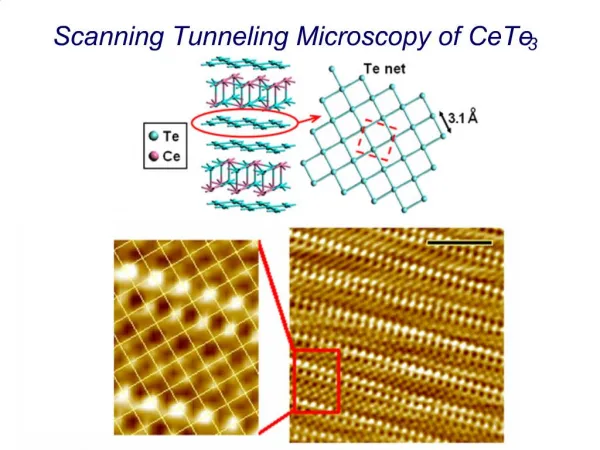
Sample; CT complex of DBA(TCNQ)2 STM Images of the DBA(TCNQ)2 Crystal Surface on Different Scales
THB on the Crystal THB condition Voltage Pulses 3 V, 300 ms 8 V, 300 ms ca. 10 nm in diameter ca. 2 nm in depth ca. 30 nm in diameter ca. 5 nm in depth
THB on the Crystal Writing Nanoscale Letters
Hole Size Depending on Voltage Condition 3~7 V, 300 ms 7 V 6 V 5 V 4 V Voltage Threshold for THB 3 V 3 V (Pulse Duration of 300 ms)
Heat to Decomposition Decomposition Temperature of DBA(TCNQ)2 177 °C The TG analysis of DBA(TCNQ)2 crystal showed a weight loss about 5.1 wt.-%, occurred between 177 and 210 °C. Maximum Temperature Rise by Voltage Pulse (Estimation) DT = 1156 K (8 V × 300 ms voltage pulse) Enough Heat for Decomposition of DBA(TCNQ)2 TG; Thermogravimetry 示差熱天秤
Verification of THB • Other Considerable Mechanisms • A Pure Surface-Conductance Change without Shape Change • AFM Imaging Confirmed the Hole Nature. • Oxidation • Both Changing the Writing Voltage Polarity and Performing under • N2 Atomsphere didn’t Affect the Formation of the Holes. • Mechanical Indentation by the STM Tip • Mechanically Formed Holes are Apparently Different from THB Holes. c) a), c) THB b), d) Mechanical Indentations c) ,d) Section analysis along the black lines shown in (a) and (b), respectively. a) b) d) AFM; Atomic Force Microscopy 原子間力顕微鏡
Summary • Nanometer-scale conductance transition was demonstrated on organic CT complexes, by applying of localized voltage pulses using STM. • The mechanism is due to localized disorder of molecules by voltage pulses. • The system using STM has a great potential for ultra-high density data storage. • THB has another possibility for nanometer-scale recording system.