Download
1 / 1
10 likes | 157 Views
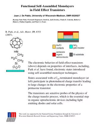
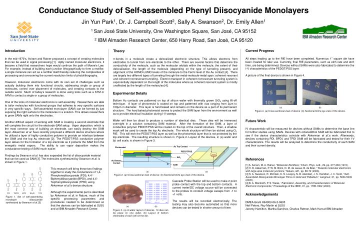
Au Top Contact. Photoresist. PEDOT/PSS. SiO 2. Au Bottom Contact. Si. SAM. (a) (b). Figure 2 . (a) Cross sectional view of device (b) Sectional bird’s eye view of the device.

E N D
Au Top Contact Photoresist PEDOT/PSS SiO2 Au Bottom Contact Si SAM (a) (b) Figure 2. (a) Cross sectional view of device (b) Sectional bird’s eye view of the device. Figure 1. Set of self-assembling monolayer diisocyanide synthesized by Swanson et al. [3] (a) (b) Figure 3. (a) A wafer layout of devices. 10 dies can be place on one wafer. (b) Layout of bottom electrodes of each cell on the die. Conductance Study of Self-assembled Phenyl Diisocyanide Monolayers Jin Yun Park1, Dr. J. Campbell Scott2, Sally A. Swanson2, Dr. Emily Allen1 1 San José State University, One Washington Square, San José, CA 95152 2 IBM Almaden Research Center, 650 Harry Road, San José, CA 95120 Current Progress All steps leading up to the RIE have been completed. Numerous 1” square die have been created for later use. Currently, final RIE parameters, such as etch rate and etch time, are being determined. Devices without SAMs were also fabricated to determine the I-V characteristics of the PEDOT/PSS layer. A picture of the final device is shown in Figure 4. Introduction In the mid-1970’s, Aviram and Ratner proposed a concept of creating molecules that can be used in signal processing [1]. Aptly named molecular electronics, it became a field that researchers hope would continue the path of Moore’s Law. For example, instead of building each junction lithographically to form a rectifier, a single molecule can act as a rectifier itself thereby reducing the complexities of processing and overcoming the current resolution limits of photolithography. However, molecular electronics come with its own set of challenges such as actually building them into functional circuits, addressing single or group of molecules, control over placement of molecules, and creating contacts to the outside world. Much of today’s research is done using tools such as a STM or AFM to contact a single or a group of molecules. One of the tools of molecular electronics is self-assembly. Researchers are able to tailor molecules with functional groups that adheres to very specific surfaces in very specific ways. Self-assembled monolayer (SAM) can be formed by just exposing the right surface to the molecules in a solution. This allows researchers to grow SAMs right onto the electrodes. Another difficult aspect of working with SAM is creating a second electrode that will complete the circuit for the electrode-SAM setup. Vapor deposition, which is the most common way of building an electrode, can easily destroy the SAM layer. Akkerman et al. have recently proposed a different device structure where he utilized a layer of highly conductive polymer to provide an interface between the SAM and the top Au electrode [2]. The PEDOT/PSS conductive polymer layer allows for the formation of a top electrode as it protects the SAM from the energetic metal vapors. The ability to use vapor deposition makes the conductance testing of SAM much easier. Findings by Swanson et al. has also expanded the list of diisocyanide material that can be used as SAM [3]. The molecules synthesized by Swanson et al. is shown in Figure 1. Theory π-bonds in a molecule create a delocalized electronic structure. This allows electrons from electrodes to tunnel from one electrode to the other. There are several factors that determine the conductivity of the molecule, such as the molecular orbitals within the molecule, the extent of their delocalization, the length of the molecule (depending on the type of tunneling present), and alignment of the HOMO-LUMO levels of the molecule to the Fermi level of the Au contact [4]. There are largely two different types of tunneling through the metal-molecule-metal span: coherent resonant and coherent nonresonant tunneling. Electron transport in coherent nonresonant tunneling system is exponentially dependent on the length of the molecules where as coherent resonant system is mostly unaffected by the length of the molecules [4]. Experimental Details Bottom Au contacts are patterned on top of silicon wafer with thermally grown SiO2 using lift-off technique. A layer of photoresist is coated on top and patterned with vias ranging from 2µm to 100µm in diameter. This layer is hard baked and remains on the device as a part of its permanent structure. The hard baked photoresist serves to protect the SAM layer from the environment as well as to provide electrical insulation during I-V sweeps. (a) (b) Figure 4. (a) Cross sectional view of device (b) Sectional bird’s eye view of the device. Future Work IV characteristic will be measured for devices without SAMs to determine the base line for further studies using SAMs. Devices with octanedithiol SAM will be fabricated first to see if the device characteristics coincide with Akkerman et al.’s work. Afterwards, devices containing PDI, BPDI, and TPDI SAM will be fabricated and tested for their I-V characteristics. The results will be analyzed to determine the conductivity of each SAM and their current density. Wafer will then be diced to produce a number of identical dies. These dies will be immersed overnight in a solution containing SAM material. After the formation of the SAM, a layer of conductive polymer PEDOT/PSS will be coated on the top of the overall structure. Then, a shadow mask will be used to create the top Au electrode. The whole structure will then be etched using O2 RIE. This will etch the PEDOT/PSS layer as well as the photoresist layer that is not protected by the top electrode. The resulting structure is shown in Figure 2. Layout of the devices, in (a) wafer and (b) cell scale, is shown in Figure 3. References [1] A. Aviram, M. A. Ratner, “Molecular Rectifiers,”Chem. Phys. Lett., 29, pp. 277-283 (1974). [2] H. B. Akkerman, P. W. M. Blom, D. M. de Leeuw, B. de Boer, “Towards molecular electronics with large-area molecular junctions,” Nature, 441, pp. 69-72 (2006). [3] S. A. Swanson, R. McClain, K. S. Lovejoy, N. B. Alamdari, J. S. Hamilton, J. C. Scott, “Self-Assembled Diisocyanide Monolayer Films on Gold and Palladium,” Langmuir, 21, pp. 5034-5039 (2005). [4] B. A. Mantooth, P. S. Weiss, “Fabrication, Assembly, and Characterization of Molecular Electronic Components,” Proceedings of the IEEE, 91, pp. 1785-1802 (2003). This research will bring these two findings together to study the conductance of 1,4-Phenylenediisocyanide (PDI), 4,4’-Biphenyldiisocyanide (BPDI), and 4,4’-Terphenyldiisocyanide (TPDI) using Akkerman et al.’s device structure. Although the experimental part is described by Akkerman et al. in Nature, much of the specific processing parameters and procedures needed to be determined so that the devices can be fabricated at SJSU and at IBM Almaden Research Center. Cascade Probe Station will be used to make 2 point probe contact with the top and bottom contacts. A current meter/DC voltage source will be connected to the probes to conduct voltage sweeps from -1 to +1 volts. The results will be recorded electronically. The testing may also become automated so that more devices can be tested in shorter amount of time. Acknowledgements DMEA Grant H94003-06-2-0605 Neil Peters, Roy Martin at SJSU Jeremy Hamilton, Martha Sanchez, Charles Rettner, Mark Hart at IBM Almaden