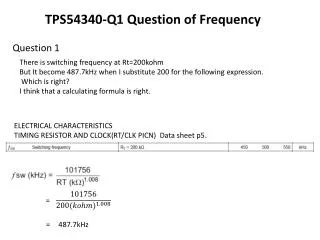
Download
1 / 11
110 likes | 303 Views
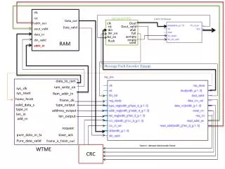
data_to_ram. ram_write_en. sys_clk. clk. sys_reset. rst. Data_out. addr_out. frame_ok. Data_valid. type_output. a out_valid. address_output. d ata_in. len_output. din_valid. RAM. General FIFO. addr_in. clk. Dout. rst. Dout_valid. din. afull. pure_data_in_tx. Wr_en. full.

E N D
data_to_ram ram_write_en sys_clk clk sys_reset rst Data_out addr_out frame_ok Data_valid type_output aout_valid address_output data_in len_output din_valid RAM General FIFO addr_in clk Dout rst Dout_valid din afull pure_data_in_tx Wr_en full Pure_data_valid frame_is_finish_out aempty Rd_en empty flush used Ram_addr_in frame_finish valid_data_s type_in len_in add_in request slave_ack WTME CRC
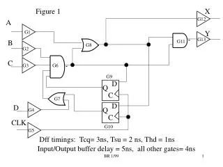
sys_clk data_to_ram sys_reset ram_write_en Add -> ADR Type ->TGA Len -> TGD valid_data_s frame_ok add type_in type_output Valid data Valid_data_s add address_output WTME type len len_output TGA_O TGA_I len add len TGD_O TGD_I pure_data_in_tx Master TX Master RX frame_finish ram_addr_in Pure_data_valid frame_is_finish_out Slave TX Slave TX Data_valid (out) Master_ack_o עולה למחזור שעון יחיד Slave Client len_in CLK_I CLK_I Data_out Data_out Slave_ack_i add_in CLK_I RST_I RST_I RST_I request Data_valid (out) ADR_O ADR_I ADR_I CLK_I type slave_ack Data_out RST_I DAT_O DAT_I DAT_I type CLK_I ADR_O RST_I add DAT_O Request-> transmit ADR_I TGA_O add WE_O DAT_I type type WE_I WE_I TGD_O type STB_O add TGA_I WE_O STB_I STB_I len len len CYC_O TGD_I STB_O CYC_I CYC_I WE_I DAT_I Wr_en CYC_O STB_I DAT_O DAT_O ACK_I Data_in DAT_I CYC_I ACK_O ACK_O ACK_I Pure_data DAT_O ACK_O
Valid_data_s = 0 Character update type_outputtype_in len_outputlen_in add_outputadd_in Request ’1’ slave_ack ’1’ Frame_ok ’1’ idel Valid_data_s = 1 Pure_data_valid=‘0’ Wait for ack Pure_data_valid= ‘1’ End transaction Transmit data temp_len = 0 Ram_write_en ’1’ Receiving data from master temp_len = 0
http://www.electronicdesignworks.com/utilities/crc_generator_doc/crc_generator_doc.htmhttp://www.electronicdesignworks.com/utilities/crc_generator_doc/crc_generator_doc.htm
WBS 1 WBM 2 Wishbone to message encoder type TX Path CRC address len Frame _finish crc Frame _OK crc Wishbone_data [7..0] UART_OUT UART TX Wishbone_data [7..0] Message encoder Data package valid busy RAM Write_enable
Filter FLASH Memory On DE2 board Altera Cyclone II FPGA CCB_disable SPANSION S29AL032D Flash Control Intercon Wishbone WBS 6 WBS 2 Wait 4M x 8 bits WBS 3 LED X 4 ADV7123 Video DAC 4WBS DISPLAY Clk 100MHz Config Control Clk 50MHz Clk & Reset Clk 65MHz WBM 3 1024 x 768@60Hz Reset WBS 5 LCD (Optional) Reset RAM HD44780 UART IN 115200 bits/sec RX PATH WBM 1 GUI MATLAB WBS 1 TX PATH WBM 2 UART OUT 115200 bits/sec
RAM data_in din_valid data_to_ram Data_out addr_in frame_ok Data_valid FIFO type_out din address_out Wr_en Dout pure_data_in_tx len_out Rd_en Dout_valid Pure_data_valid frame_finish valid_data_s Ram_addr_in type_in len_in add_in request WTME CRC
sys_clk data_to_ram sys_reset ram_write_en Add -> ADR Type ->TGA Len -> TGD valid_data_s frame_ok add type_in type_output Valid data Valid_data_s add address_output WTME type len len_output TGA_O TGA_I len add len TGD_O TGD_I pure_data_in_tx Master TX Master RX frame_finish ram_addr_in Pure_data_valid frame_is_finish_out Slave TX Slave TX Data_valid (out) Master_ack_o עולה למחזור שעון יחיד Slave Client len_in CLK_I CLK_I Data_out Data_out Slave_ack_i add_in CLK_I RST_I RST_I RST_I request Data_valid (out) ADR_O ADR_I ADR_I CLK_I type slave_ack Data_out RST_I DAT_O DAT_I DAT_I type CLK_I ADR_O RST_I add DAT_O Request-> transmit ADR_I TGA_O add WE_O DAT_I type type WE_I WE_I TGD_O type STB_O add TGA_I WE_O STB_I STB_I len len len CYC_O TGD_I STB_O CYC_I CYC_I WE_I DAT_I Wr_en CYC_O STB_I DAT_O DAT_O ACK_I Data_in DAT_I CYC_I ACK_O ACK_O ACK_I Pure_data DAT_O ACK_O
RAM data_in din_valid CRC data_to_ram Data_out addr_in dout frame_ok Data_valid FIFO type_out din din address_out din_valid Wr_en Dout pure_data_in_tx Data_crc len_out Rd_en Dout_valid Pure_data_valid UART din dout Reg_ready Mp_encoder frame_finish type_reg valid_data_s Ram_addr_in len_reg type_in add_reg len_in Dout_valid add_in Crc_in WTME
WBS 1 WBM 2 Wishbone to message encoder type TX Path CRC address len Frame _finish crc Frame _OK crc Wishbone_data [7..0] UART_OUT UART TX Wishbone_data [7..0] Message encoder Data package valid busy RAM Write_enable
Valid_data_s = 0 Character update idel Valid_data_s = 1 Pure_data_valid=‘0’ Wait for ack Pure_data_valid= ‘1’ End transaction Transmit data temp_len!= 0 temp_len = 0