Download
1 / 52
520 likes | 624 Views
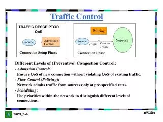
Dynamic Traffic Control. Group 2 Chun Han Chen Timothy Kwan Tom Bolds Shang Yi Lin Manager Randal Hong. Project Objective : Dynamic Control of Traffic Lights. Wed. Dec. 3. Presentation Outline. Marketing Project Description Design Process Floor Plan Evolution Layout

E N D
Dynamic Traffic Control Group 2 Chun Han Chen Timothy Kwan Tom Bolds Shang Yi Lin Manager Randal Hong Project Objective : Dynamic Control of Traffic Lights Wed. Dec. 3
Presentation Outline • Marketing • Project Description • Design Process • Floor Plan Evolution • Layout • Verification • Issues Encountered • Specifications
Marketing / Description Tom Bolds
Current System • The current system has sensors that detects cars leaving their lanes • Induction loops under the pavement • Video cameras • Depending on the time of day, the intersection lets each arm go for a set amount of time • If no cars are present in one arm, the other arm is green • It cannot learn or adapt • Cost for entire system: $35,000
A Better System • This system detects cars entering and leaving each arm • The time that an arm is green is determined in part, by past traffic • Exceptional traffic flow will change the system immediately • Cost for entire system: $24,000
Market • 4 Million traffic lights in the US • A few user inputs lets the system be adjustable for different situations • Roads of different sizes • Different space constraints • Price goes down and quality goes up
Goals • When the government is involved, cost needs to be low • Only 4 metal layers used • Optimized for small size • Could have gone the “all pseudo-nmos” route • We don’t want to use megawatts on a traffic light • Cmos logic to minimize size and power consumption
Goals • Even if it causes just a few accidents nobody will buy it, and we get sued • Design needs to be robust • Handle power failures • Return to a known state • Predictable behavior • People are used to driving a certain way • No accidental switching • Minimum time for lights to change
Installation • The only change necessary would be the detectors for entering/leaving cars • Current system has ground sensors or video camera to detect the first car at an intersection • Could add another detector farther back, or use video/sound detection to determine where cars are
Traffic Flow Sensors (Blue) To detect the car entered Sensors (Red) To detect the car leaved
Traffic Light Flow Phase C PED ARM 1 Red Green (Straight + Right) Y Red+Green(Left) Y Red Green Y Red Green (Straight + Right) Y Red+Green(Left) Y ARM 2 Phase A Phase B Phase A Phase B ARM1 ARM1 ARM2 ARM2 We define three phases (A,B,C) for different operations. Whenever pedestrian push the button, then this light will insert in the end of this cycle.
reset Pedestrian For Green light Control Hold until n1 or n2 changes For Pedestrian For Red + Left Light favors n1 or n2 ? Yes Yes No Light favors arm1 or arm2 ? n1 n2 T>= Rp ? Yes Yes T<r1? T<r2? n1 n2 Reset T = 0 No No T<rleft? Yes T<rleft? Yes T>= R1? T>= R2? No No Yes Yes No No n1 not change in T = 5? Yes n2 not change in T = 5? Yes Yes n2=0? n1=0? No No No No No Yes Yes T>= Rleft? T>= Rleft? Yes Yes No f2<=0? f1<=0? No No Switch Light n1, n2 :# of cars T :Time spent in this phase Ri , ri : Max. and Min. time for each phase fi : the control function f1 = α1*n1+ β1 – n2 f2 = α2*n2+ β2 – n1
Choose the Phase Initial Init. Ped = 0 SW = 0 SW =0 ARM = 0 ARM = 1 G.R R.G SW = 1 SW = 1 T = 2 PED = 0 T = 2 PED = 0 SW – Switch light G – Green R – Red Y – Yellow T – Time for Yellow PED – Pedestrian T < 2 Y.R R.Y T < 2 T = 2 T = 2 SW = 0 R+Left.R R.R+Left SW =0 SW = 1 SW = 1 SW = 1 T<= 2 Y.R R.Y T<= 2 SW (1bit) PED = 1 T = 2 PED = 1 T = 2 ARM (1bit) PED FSM Phase(2bits) PED(1bit) T (2bits) SW = 0
Learning? • The way we learn is by changing beta • To take out the division, multiply everything else by Qlen • We are actually calculating f*Qlen, but it works since it only matters if it’s < 0
2:1 MUX 110 Reg X 10 β 110 11 11 X 10 Reg X 10 11 2:1 MUX 11 1 1 ARM 11 11 ARM 11 16:1 MUX 1 1 1:16 De-MUX ROM 11 q0,q1: X 2 n0 Dot Lint to FSM 11 Shifting n1 n0 = 0 11 11 X 9 β n0 ENTER 11 11 n1 β n1 = 0 11 q0 11 q1 F F <= 0 12 Accum 11 Reg 11 11 Q_len 11 bit ½ 11 Reg X 9 12 bit Reg X1 n_avg 11 4 s0,s1: X 2 Sel ALU 11 11 X 1 OUT / LEFT 11 12 111 11 s0 αn0-n1 11 s1 αn0 Accum 11 Reg 11 11 α0 q0-s0 11 α1 11 q1-s1 N_avg Q(αn0-n1) αn0-n1 αn0 11 2:1 MUX α0,α1: X 2 q0-s0 4 User Input q1-s1 11 11 11 Reg Q(αn0-n1) Sel ROM 2 4 Sel_ALU Sel 8 X 8 : Dot Line to Comparator R,r, RL,rl for Arm1 Arm2 2:1 MUX 8 X 8 8X8 User Input R,r 11 Reg 8X8 11 11 ½ ROM 11 11 11 11 User Input Q 11 11 Reg 11 8 : 1 MUX Trigger, when cars go left turn System Clock 1 1 Sel_D 2 ARM 1 System Clock R & r, R_L& r_L 2 Sel_ALU 1 8 8 8 X 8 3 Sel_C 2 ARM 2 8 Clk Div. Accmu Reg 4X3 Sel FSM FSM 1 1 PED INT. Compar SW 1 8 8 3 1 ARM 1 Accmu Reg Left-Turn Counter 8 Sel_C PED 1 Complete n0 1 Shifting 8 n1 CLK 1 8 F 8 T 1 Clear 1 1 Ser_D 2 : 1 MUX Operation Data Input Initial Values Selection R, r, R_L, r_l Light Control FSM Flow Control FSM Clock T, Left-Turn Counter
Design Process Shang-Yi Lin
Design Process – Objective • Goal - Compact Area - Low Power • Trade-Off - Performance
Design Process - Overview Behaviors / Flow Charts Behavior Verilog / JAVA Structural Verilog / Structure Schematic / Cadence Layout / Virtuso Extracted RC / Simulation
Design Process – Behaviors • Finalize Chip Functionality - Make behaviors, function clear • Feasible & Reasonable Algorithm - Complex & Fast != Good Design Order of Traffic Light Traffic Light FSM Flow Control FSM
Design Process – Verilog / JAVA • Behavior Verilog & JAVA
Design Process – Structure • Block Diagram : • Behavior Verilog to Structural Verilog • Data path and function blocks are determined • Initiate Floorplan • Floor Plan : - Routing Issue • Re-Use of Components : • Decrease Chip Area
Design Process – Schematic • Compact Design : - Minimize transistor count • Transistor Sizing : • Minimize transistor size • Equivalent Pull-Up & Pull-Down ability • Implementation: • Put reasonable output loads for simulation • Sized buffers for global control signals
Design Process – Layout • Defined the Metal Directionality : • M1 & M2 : Local, power rails • M3 & M4 : Global, Control, Clock • Special Case : Depended • Focus on Compact Layout: • Floor plan keeps updating • Consider the interconnect between blocks • Global Routing: • Fixed height for most blocks • Use wider global wires • Leave wiring space
Design Process – Extract RC • Block Level • Extracted RC simulation for each block • Combine multiple blocks to simulate • Chip Level • Ensure global signals integrity • Whole chip simulation
Floorplan Evolution Shang-Yi Lin
Floor Plan • First Version • Block Diagram • Sample Layout Size • Routing Issue • Re-Use Components 13.5 16.6 6.5 6.6 2X1 MUX Register (1bit)
Floor Plan – 1st Version Input Get q0 q1 s0 s1 Input PED, CLK Give R,r Avg. q Reuse Control Light Compare T ½ , Q_L F , Ni FPU Output
Floor Plan – Update • Structure : Logic components are determined
Floor Plan – Update • Layout : Refined Function Block
Refined Layout • More Precise Layout Shape & Size
Layout / Verification Chun Han Chen
Layout - ALU Input Output
Layout – FSMs Timing Control FSM Light Control FSM
Layout – Memory Devices & Interconnection Parts Counters Shift Registers and MUXs Counters Shift Registers MUX Counters Shift Registers 2:1 MUX
Layout – Memory Devices & Interconnection Parts 11-bits 16:1 MUX Input Select Output
Layout – Memory Devices & Interconnection Parts Output to Timing Control FSM Real time counter, MUX, and, Comparator
Layout – Memory Devices & Interconnection Parts Control + Registers Control Logic Input from ALU Output
Verification – Methodology Functionality Validation -Java V.S. Behavioral Verilog -Behavioral Verilog V.S. Structural Verilog Schematic Checks -Structure Verilog V.S. Schematic Layout Verification 1.Whole chip extracted RC simulation by using Ultrasim 2.Comparing the results with schematic simulation 3.Separated simulations for pedestrian signal
Verification – Methodology Extracted RC for the whole chip
Verification – Light Switching Switch Continue
Specification Issues Encountered Timothy Kwan
Specifications • Area = .146270 mm2 • 498.69 x 293.31 um^2 • 1:1.7002 Aspect Ratio • Transistors 18834 Total • 8613 pmos • 10221 nmos • Density • .1288 transistors / um^2 • Speed • 10 MHz • I/O’s • 74 inputs • 5 outputs
Issues Encountered • Muxzilla • Large consecutive pass transistor muxes • Floor plan • Increasing number of transistors led to larger blocks • 12000 => 18834 • Wire Routing • Metal Directionality • Large Number of Wires • I/Os • Complicated FSM Logic and glitches


![[M2] Traffic Control](https://cdn1.slideserve.com/3370967/m2-traffic-control-dt.jpg)


![[M2] Traffic Control](https://cdn2.slideserve.com/4578602/m2-traffic-control-dt.jpg)